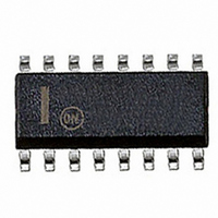
MC74HC4538ADG ON Semiconductor, MC74HC4538ADG Datasheet - Page 11

MC74HC4538ADG
Manufacturer Part Number
MC74HC4538ADG
Description
IC MULTIVIBRATOR DUAL 16-SOIC
Manufacturer
ON Semiconductor
Series
74HCr
Specifications of MC74HC4538ADG
Logic Type
Monostable
Independent Circuits
2
Schmitt Trigger Input
No
Propagation Delay
30ns
Current - Output High, Low
5.2mA, 5.2mA
Voltage - Supply
3 V ~ 6 V
Operating Temperature
-55°C ~ 125°C
Mounting Type
Surface Mount
Package / Case
16-SOIC (3.9mm Width)
Elements Per Chip
2
Logic Family
HC
Input Bias Current (max)
0.13 mA
Propagation Delay Time
195 ns, 39 ns, 33 ns
High Level Output Current
- 5.2 mA
Low Level Output Current
5.2 mA
Supply Voltage (max)
6 V
Supply Voltage (min)
3 V
Maximum Operating Temperature
+ 125 C
Minimum Operating Temperature
- 55 C
Mounting Style
SMD/SMT
Operating Supply Voltage
3.3 V, 5 V
Circuit Type
Low-Power Schottky
Current, Supply
800 μA
Function Type
2-Channels
Logic Function
Multivibrator
Number Of Circuits
Dual
Package Type
SOIC-16
Special Features
Retriggerable/Resettable Monostable
Temperature, Operating, Range
-55 to +125 °C
Voltage, Supply
3 to 6 V
Lead Free Status / RoHS Status
Lead free / RoHS Compliant
Other names
MC74HC4538ADG
MC74HC4538ADGOS
MC74HC4538ADGOS
reference circuit (#17), the output of the upper reference
circuit goes low (#18). This causes the output latch to toggle,
taking the Q output of the HC4538A to a low state (#19), and
completing the time−out cycle.
POWER−DOWN CONSIDERATIONS
down the HC4538A because of the amount of energy stored
in the capacitor. When a system containing this device is
powered down, the capacitor may discharge from V
through the input protection diodes at pin 2 or pin 14.
Current through the protection diodes must be limited to 30
mA; therefore, the turn−off time of the V
must not be faster than t = V
if V
no faster than t = (5.0 V)(15 mF)/30 mA = 2.5 ms. This is
usually not a problem because power supplies are heavily
filtered and cannot discharge at this rate.
the HC4538A may sustain damage. To avoid this possibility,
use an external damping diode, D
Figure 11. Best results can be achieved if diode D
to be a germanium or Schottky type diode able to withstand
large current surges.
RESET AND POWER ON RESET OPERATION
Q output of the HC4538A to a low state.
occurs (#20) while C
voltage of the upper reference circuit (#21). When a reset
When C
Large values of C
When a more rapid decrease of V
A low voltage applied to the Reset pin always forces the
The timing diagram illustrates the case in which reset
CC
= 5.0 V and C
x
charges up to the reference voltage of the upper
x
x
x
may cause problems when powering
= 15 mF, the V
is charging up toward the reference
CC
C
Figure 13. Discharge Protection During Power Down
x
x
, connected as shown in
/(30 mA). For example,
CC
CC
to zero volts occurs,
supply must turn off
CC
A
B
power supply
x
is chosen
http://onsemi.com
MC74HC4538A
RESET
C
CC
X
11
occurs, the output of the reset latch goes low (#22), turning
on transistor M1. Thus C
V
will be high causing a reset condition. This will prevent the
trigger−control circuit from accepting a trigger input during
this state. The HC4538A’s Q outputs are low and the Q not
outputs are high.
RETRIGGER OPERATION
HC4538A may be retriggered during timing out of the
output pulse at any time after the trigger−control circuit
flip−flop has been reset (#24), and the voltage across C
above the lower reference voltage. As long as the C
is below the lower reference voltage, the reset of the
flip−flop is high, disabling any trigger pulse. This prevents
M3 from turning on during this period resulting in an output
pulse width that is predictable.
trigger mode is a function of loop delay, M3 conductivity,
and V
function of 1) time to discharge R
reference voltage (T
time to charge R
lower reference voltage (T
non−retriggerable mode.
(AN1558/D) titled Characterization of Retrigger Time in
the HC4538A Dual Precision Monostable Multivibrator.
D
R
CC
On power up of the HC4538A the power−on reset circuit
When used in the retriggerable mode (Figure 12), the
The amount of undershoot voltage on R
Figure 13 shows the device configured in the
For additional information, please see Application Note
X
X
(#23) to await the next trigger signal.
DD
Q
Q
. Minimum retrigger time, trr (Figure 7), is a
V
CC
x
C
x
from the undershoot voltage back to the
discharge
x
is allowed to quickly charge up to
charge
); 2) loop delay (T
).
x
C
x
from V
x
C
x
DD
during the
delay
x
to lower
voltage
); 3)
x
is


