N74F280BN,602 NXP Semiconductors, N74F280BN,602 Datasheet - Page 2
N74F280BN,602
Manufacturer Part Number
N74F280BN,602
Description
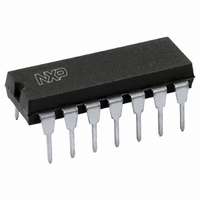
IC PARITY GEN/CHKER 9BIT 14DIP
Manufacturer
NXP Semiconductors
Series
74Fr
Datasheet
1.N74F280BD623.pdf
(8 pages)
Specifications of N74F280BN,602
Number Of Circuits
9-Bit
Package / Case
14-DIP (0.300", 7.62mm)
Logic Type
Parity Generator/Checker
Current - Output High, Low
1mA, 20mA
Voltage - Supply
4.5 V ~ 5.5 V
Operating Temperature
-40°C ~ 85°C
Mounting Type
Through Hole
Number Of Bits
9
Logic Family
F
High Level Output Current
- 1 mA
Low Level Output Current
20 mA
Propagation Delay Time
10 ns @ 5 V
Operating Supply Voltage
5 V
Maximum Operating Temperature
+ 70 C
Minimum Operating Temperature
0 C
Mounting Style
Through Hole
Supply Voltage (max)
5.5 V
Supply Voltage (min)
4.5 V
Logical Function
Parity Gen/Checker
Number Of Elements
1
Operating Supply Voltage (typ)
5V
Package Type
PDIP
Operating Temp Range
0C to 70C
Operating Supply Voltage (min)
4.5V
Operating Supply Voltage (max)
5.5V
Pin Count
14
Mounting
Through Hole
Operating Temperature Classification
Commercial
Technology
Bipolar
Lead Free Status / RoHS Status
Lead free / RoHS Compliant
Lead Free Status / RoHS Status
Lead free / RoHS Compliant, Lead free / RoHS Compliant
Other names
933829000602
N74F280BN
N74F280BN
N74F280BN
N74F280BN


Philips Semiconductors
FEATURES
DESCRIPTION
The 74F280B is a 9-bit Parity Generator or Checker commonly used
to detect errors in high speed data transmission or data retrieval
systems. Both Even (
for generating or checking even or odd parity on up to 9 bits.
The Even (
inputs (I
odd number of Data inputs are High.
Expansion to larger word sizes is accomplished by tying the Even
(
final stage. This expansion scheme allows an 81-bit data word to be
checked in less than 20ns.
ORDERING INFORMATION
INPUT AND OUTPUT LOADING AND FAN-OUT TABLE
NOTE:
One (1.0) FAST Unit Load is defined as: 20 A in the High state and 0.6mA in the Low state.
LOGIC SYMBOL
1996 Mar 12
High-impedance NPN base inputs for reduced loading
(20 A in Low and High states)
Buffered inputs — one normalized load
Word length easily expanded by cascading
Industrial temperature range available (–40 C to +85 C)
E
9-bit odd/even parity generator/checker
) outputs of up to nine parallel devices to the data inputs of the
14-pin plastic DIP
14-pin plastic SO
0
DESCRIPTION
- I
8
E
) are High. The Odd (
) parity output is High when an even number of Data
PINS
I
0
E
,
- I
8
O
I
8
0
E
I
9
) and Odd (
1
10 11 12 13
I
2
5
I
E
3
I
4
O
) parity output is High when an
O
I
5
) parity outputs are available
6
O
COMMERCIAL RANGE
I
1
6
T
amb
SF00845
V
I
2
7
CC
N74F280BN
N74F280BD
DESCRIPTION
= 0 C to +70 C
I
Parity outputs
4
8
= 5V 10%,
Data inputs
2
PIN CONFIGURATION
IEC/IEEE SYMBOL
74F280B
V
GND=Pin 7
CC
TYPE
T
INDUSTRIAL RANGE
amb
=Pin 14
V
CC
= –40 C to +85 C
I74F280BN
I74F280BD
HIGH/LOW
= 5V 10%,
74F(U.L.)
1.0/0.033
50/33
PROPAGATION
GND
TYPICAL
NC
DELAY
10
11
12
13
I
I
I
O
E
6
7
8
8
9
1
2
4
5.5ns
1
2
3
4
5
6
7
2K
SF00849
O
E
SF00846
14
13
12
10
11
9
8
SUPPLY CURRENT
LOAD VALUE
PKG. DWG. #
1.0mA/20mA
HIGH/LOW
20 A/20 A
Product specification
V
I
I
I
I
I
I
5
4
3
2
1
0
SOT108-1
SOT27-1
CC
TYPICAL
(TOTAL)
5
6
74F280B
26mA
853-0363 16555
Related parts for N74F280BN,602
Image
Part Number
Description
Manufacturer
Datasheet
Request
R

Part Number:
Description:
NXP Semiconductors designed the LPC2420/2460 microcontroller around a 16-bit/32-bitARM7TDMI-S CPU core with real-time debug interfaces that include both JTAG andembedded trace
Manufacturer:
NXP Semiconductors
Datasheet:

Part Number:
Description:
NXP Semiconductors designed the LPC2458 microcontroller around a 16-bit/32-bitARM7TDMI-S CPU core with real-time debug interfaces that include both JTAG andembedded trace
Manufacturer:
NXP Semiconductors
Datasheet:
Part Number:
Description:
NXP Semiconductors designed the LPC2468 microcontroller around a 16-bit/32-bitARM7TDMI-S CPU core with real-time debug interfaces that include both JTAG andembedded trace
Manufacturer:
NXP Semiconductors
Datasheet:
Part Number:
Description:
NXP Semiconductors designed the LPC2470 microcontroller, powered by theARM7TDMI-S core, to be a highly integrated microcontroller for a wide range ofapplications that require advanced communications and high quality graphic displays
Manufacturer:
NXP Semiconductors
Datasheet:
Part Number:
Description:
NXP Semiconductors designed the LPC2478 microcontroller, powered by theARM7TDMI-S core, to be a highly integrated microcontroller for a wide range ofapplications that require advanced communications and high quality graphic displays
Manufacturer:
NXP Semiconductors
Datasheet:
Part Number:
Description:
The Philips Semiconductors XA (eXtended Architecture) family of 16-bit single-chip microcontrollers is powerful enough to easily handle the requirements of high performance embedded applications, yet inexpensive enough to compete in the market for hi
Manufacturer:
NXP Semiconductors
Datasheet:
Part Number:
Description:
The XA-S3 device is a member of Philips Semiconductors? XA(eXtended Architecture) family of high performance 16-bitsingle-chip microcontrollers
Manufacturer:
NXP Semiconductors
Datasheet:

Part Number:
Description:
The NXP BlueStreak LH75401/LH75411 family consists of two low-cost 16/32-bit System-on-Chip (SoC) devices
Manufacturer:
NXP Semiconductors
Datasheet:
Part Number:
Description:
The NXP LPC3130/3131 combine an 180 MHz ARM926EJ-S CPU core, high-speed USB2
Manufacturer:
NXP Semiconductors
Datasheet:
Part Number:
Description:
The NXP LPC3141 combine a 270 MHz ARM926EJ-S CPU core, High-speed USB 2
Manufacturer:
NXP Semiconductors
Part Number:
Description:
The NXP LPC3143 combine a 270 MHz ARM926EJ-S CPU core, High-speed USB 2
Manufacturer:
NXP Semiconductors

Part Number:
Description:
The NXP LPC3152 combines an 180 MHz ARM926EJ-S CPU core, High-speed USB 2
Manufacturer:
NXP Semiconductors
Part Number:
Description:
The NXP LPC3154 combines an 180 MHz ARM926EJ-S CPU core, High-speed USB 2
Manufacturer:
NXP Semiconductors

Part Number:
Description:
Standard level N-channel enhancement mode Field-Effect Transistor (FET) in a plastic package using NXP High-Performance Automotive (HPA) TrenchMOS technology
Manufacturer:
NXP Semiconductors
Datasheet: