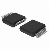
74LV4094DB,112 NXP Semiconductors, 74LV4094DB,112 Datasheet - Page 10

74LV4094DB,112
Manufacturer Part Number
74LV4094DB,112
Description
IC 8ST SHIFT/STORE BUS 16-SSOP
Manufacturer
NXP Semiconductors
Series
74LVr
Datasheet
1.74LV4094DB112.pdf
(21 pages)
Specifications of 74LV4094DB,112
Package / Case
16-SSOP
Logic Type
Shift Register
Output Type
Standard
Function
Serial to Parallel
Number Of Elements
1
Number Of Bits Per Element
8
Voltage - Supply
1 V ~ 3.6 V
Operating Temperature
-40°C ~ 125°C
Mounting Type
Surface Mount
Counting Sequence
Serial to Serial/Parallel
Number Of Circuits
1
Logic Family
74LV
Propagation Delay Time
115 ns
Supply Voltage (max)
3.6 V
Maximum Operating Temperature
+ 125 C
Minimum Operating Temperature
- 40 C
Mounting Style
SMD/SMT
Operating Supply Voltage
1 V to 3.6 V
Lead Free Status / RoHS Status
Lead free / RoHS Compliant
Lead Free Status / RoHS Status
Lead free / RoHS Compliant, Lead free / RoHS Compliant
Other names
568-2977-5
935166090112
935166090112
NXP Semiconductors
Table 7.
Voltages are referenced to GND (ground = 0 V); C
[1]
[2]
[3]
[4]
[5]
[6]
[7]
12. Waveforms
74LV4094
Product data sheet
Symbol
C
Fig 8.
PD
All typical values are measured at T
All typical values are measured at V
t
t
t
t
C
P
f
f
C
V
N = number of inputs switching;
∑(C
pd
en
dis
t
i
o
D
CC
PD
= input frequency in MHz;
L
is the same as t
= output frequency in MHz;
is the same as t
is the same as t
= output load capacitance in pF;
= C
is the same as t
L
is used to determine the dynamic power dissipation (P
= supply voltage in V;
× V
Measurement points are given in
V
Propagation delay input (CP) to output (QPn, QS1, QS2), output transition time, clock input (CP) pulse
width and the maximum frequency (CP)
PD
OL
Dynamic characteristics
Parameter
power
dissipation
capacitance
CC
× V
and V
2
× f
CC
o
2
) = sum of outputs.
OH
× f
THL
PLH
PZH
PLZ
i
are typical voltage output levels that occur with the output load.
× N + ∑(C
and t
and t
and t
and t
TLH
QPn, QS1 output
Conditions
C
V
PHL
PZL
PHZ
I
.
L
= GND to V
L
.
.
= 50 pF; f = 1 MHz;
.
QS2 output
× V
CP input
amb
CC
CC
2
…continued
= 3.3 V.
= 25 °C.
× f
Table
o
GND
All information provided in this document is subject to legal disclaimers.
V
V
) where:
V
V
CC
OH
OH
OL
OL
V
8.
I
L
Rev. 3 — 7 March 2011
= 50 pF unless otherwise specified; for test circuit see
V
t
M
PLH
D
t
W
in μW).
V
1/f
M
max
[7]
t
PLH
Min
-
V
−40 °C to 85 °C
M
t
PHL
Typ
83
[1]
8-stage shift-and-store bus register
t
Max
PHL
-
001aaf113
−40 °C to +125 °C
Min
-
74LV4094
© NXP B.V. 2011. All rights reserved.
Figure
Max
-
12.
10 of 21
Unit
pF


