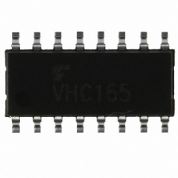
TC74VHC165FN(F,M) Toshiba, TC74VHC165FN(F,M) Datasheet

TC74VHC165FN(F,M)
Specifications of TC74VHC165FN(F,M)
Related parts for TC74VHC165FN(F,M)
TC74VHC165FN(F,M) Summary of contents
Page 1
... TOSHIBA CMOS Digital Integrated Circuit Silicon Monolithic TC74VHC165F,TC74VHC165FN,TC74VHC165FT,TC74VHC165FK 8-Bit Shift Register (P-IN, S-OUT) The TC74VHC165 is an advanced high speed CMOS 8-BIT PARALLEL/SERIAL-IN, SERIAL-OUT SHIFT REGISTER fabricated with silicon gate C MOS technology achieves the high speed operation similar to equivalent Bipolar Schottky TTL while maintaining the CMOS low power dissipation. ...
Page 2
Pin Assignment GND 8 Truth Table Inputs SHIFT/ CK SERIAL CK LOAD INH ...
Page 3
Timing Chart CK CK INH Serial Input Shift/ LOAD Parallel Inputs Output QH Output INHIBIT SERIAL SHIFT LOAD 3 TC74VHC165F/FN/FT/FK ...
Page 4
System Diagram SERIAL INPUT 10 CLOCK 2 15 CLOCK INHIBIT 1 SHIFT/ LOAD Absolute Maximum Ratings (Note) Characteristics Supply voltage range DC input voltage DC output voltage Input diode current Output diode current DC output current DC V /ground current ...
Page 5
Recommended Operating Conditions (Note) Characteristics Supply voltage Input voltage Output voltage Operating temperature Input rise and fall time Note: The recommended operating conditions are required to ensure the normal operation of the device. Unused inputs must be tied to either ...
Page 6
Timing Requirements (input: t Characteristics Symbol Minimum pulse width (CK, CK INH) Minimum pulse width ( Minimum set-up time (PI Minimum set-up time (SI-CK, CK INH) Minimum set-up time ( S/ -CK, CK INH) ...
Page 7
AC Characteristics (input: t Characteristics Symbol Propagation delay time t pLH (CK, CK INH-QH pHL Propagation delay time t pLH ( S/ -QH pHL Propagation delay time t pLH (H-QH, Q ...
Page 8
Package Dimensions Weight: 0.18 g (typ.) TC74VHC165F/FN/FT/FK 8 2006-06-01 ...
Page 9
Package Dimensions Weight: 0.18 g (typ.) TC74VHC165F/FN/FT/FK 9 2006-06-01 ...
Page 10
Package Dimensions (Note) Note: This package is not available in Japan. Weight: 0.13 g (typ.) TC74VHC165F/FN/FT/FK 10 2006-06-01 ...
Page 11
Package Dimensions Weight: 0.06 g (typ.) TC74VHC165F/FN/FT/FK 11 2006-06-01 ...
Page 12
Package Dimensions Weight: 0.02 g (typ.) TC74VHC165F/FN/FT/FK 12 2006-06-01 ...
Page 13
... The information contained herein is presented only as a guide for the applications of our products. No responsibility is assumed by TOSHIBA for any infringements of patents or other rights of the third parties which may result from its use. No license is granted by implication or otherwise under any patents or other rights of TOSHIBA or the third parties. • ...


