74LV165AD,118 NXP Semiconductors, 74LV165AD,118 Datasheet - Page 7
74LV165AD,118
Manufacturer Part Number
74LV165AD,118
Description
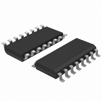
IC 8BIT SHIFT REGISTER 16SOIC
Manufacturer
NXP Semiconductors
Series
74LVr
Specifications of 74LV165AD,118
Package / Case
16-SOIC (3.9mm Width)
Logic Type
Shift Register
Function
Parallel or Serial to Serial
Output Type
Differential
Number Of Elements
1
Number Of Bits Per Element
8
Voltage - Supply
1 V ~ 5.5 V
Operating Temperature
-40°C ~ 125°C
Mounting Type
Surface Mount
Counting Sequence
Serial/Parallel to Serial
Number Of Circuits
1
Logic Family
LV
Propagation Delay Time
7.5 ns
Supply Voltage (max)
5.5 V
Maximum Operating Temperature
+ 85 C
Minimum Operating Temperature
- 40 C
Mounting Style
SMD/SMT
Operating Supply Voltage
2.5 V, 3.3 V, 5 V
Supply Voltage (min)
2 V
Lead Free Status / RoHS Status
Lead free / RoHS Compliant
Lead Free Status / RoHS Status
Lead free / RoHS Compliant, Lead free / RoHS Compliant
Other names
74LV165AD-T
74LV165AD-T
935273176118
74LV165AD-T
935273176118
Available stocks
Company
Part Number
Manufacturer
Quantity
Price
Company:

Part Number:
74LV165AD,118
Manufacturer:
NXP Semiconductors
Quantity:
2 000


1. Unless otherwise stated, all typical values are measured at T
2. Typical values are measured at V
Philips Semiconductors
AC CHARACTERISTICS ( Continued )
GND = 0V; t
NOTES:
AC WAVEFORMS
V
V
V
output load.
Note to Figures 1 and 2
The changing to output assumes internal Q
1998 May 07
Figure 1. Clock (CP) to output (Q
SYMBOL
SYMBOL
M
M
OL
8-bit parallel-in/serial-out shift register
= 1.5 V at V
= 0.5
The changing to output assumes internal Q
the clock pulse width and the maximum clock frequency.
f
f
and V
max
t
su
t
t
h
h
CP INPUT
OUTPUT
Q
7
OH
or Q
V
GND
V
V
r
CC
OH
OL
= t
are the typical output voltage drop that occur with the
V
7
I
Set-up time
D
D
Hold time
Hold time
D
D to PL
D
Hold time
Hold time
CE to CP,
CP t CE
CP to CE
Maximum clock
pulse frequency
CC
at V
f
n
n
s
n
PARAMETER
PARAMETER
to PL
to PL
to CP, CE
to PL
2.5ns; C
CC
2.7 V.
V
M
t
PHL
2.7 V;
t
W
L
= 50pF; R
1/f
V
M
max
6
CC
7
opposite state from Q
WAVEFORM
WAVEFORM
or Q
L
Figures 1, 2
Figures 1, 2
Figures 1, 2
Figures 1 2
Figures 1, 2
= 3.3 V.
= 1K
6
opposite state from Q
7
) propagation delays,
t
PLH
7
.
SV00590
7
CONDITION
amb
.
3.0 to 3.6
4.5 to 5.5
3.0 to 3.6
4.5 to 5.5
3.0 to 3.6
4.5 to 5.5
3.0 to 3.6
4.5 to 5.5
V
CC
1.2
2.0
2.7
1.2
2.0
2.7
1.2
2.0
2.7
2.0
2.7
= 25 C
(V)
7
output (Q
Q
7
Figure 2. Parallel load (PL) pulse width, the parallel load to
The changing to output assumes internal Q
or Q
CE, CP INPUT
7
PL INPUT
OUTPUT
7
GND
GND
V
V
(CP) and clock enable (CE) removal time.
or Q
MIN
22
16
13
22
16
13
14
19
24
36
OH
OL
V
V
–
9
–
9
–
5
5
5
5
I
I
7
–40 to +85 C
) propagation delays, the parallel load to clock
TYP
–30
–5
65
25
5
20
–8
–6
–4
40
60
75
8
6
4
7
5
4
3
2
V
2
2
M
1
t
PHL
t
W
MAX
–
–
–
–
–
–
–
–
–
–
–
–
–
–
–
–
–
–
–
6
opposite state from Q
V
M
–40 to +125 C
MIN
t
rem
26
19
15
10
26
19
15
10
12
16
20
30
–
–
–
5
5
5
5
V
Product specification
M
MAX
74LV165
–
–
–
–
–
–
–
–
–
–
–
–
–
–
–
–
–
–
–
7
.
SV00591
UNIT
UNIT
MHz
MHz
ns
ns
ns
Related parts for 74LV165AD,118
Image
Part Number
Description
Manufacturer
Datasheet
Request
R

Part Number:
Description:
NXP Semiconductors designed the LPC2420/2460 microcontroller around a 16-bit/32-bitARM7TDMI-S CPU core with real-time debug interfaces that include both JTAG andembedded trace
Manufacturer:
NXP Semiconductors
Datasheet:

Part Number:
Description:
NXP Semiconductors designed the LPC2458 microcontroller around a 16-bit/32-bitARM7TDMI-S CPU core with real-time debug interfaces that include both JTAG andembedded trace
Manufacturer:
NXP Semiconductors
Datasheet:
Part Number:
Description:
NXP Semiconductors designed the LPC2468 microcontroller around a 16-bit/32-bitARM7TDMI-S CPU core with real-time debug interfaces that include both JTAG andembedded trace
Manufacturer:
NXP Semiconductors
Datasheet:
Part Number:
Description:
NXP Semiconductors designed the LPC2470 microcontroller, powered by theARM7TDMI-S core, to be a highly integrated microcontroller for a wide range ofapplications that require advanced communications and high quality graphic displays
Manufacturer:
NXP Semiconductors
Datasheet:
Part Number:
Description:
NXP Semiconductors designed the LPC2478 microcontroller, powered by theARM7TDMI-S core, to be a highly integrated microcontroller for a wide range ofapplications that require advanced communications and high quality graphic displays
Manufacturer:
NXP Semiconductors
Datasheet:
Part Number:
Description:
The Philips Semiconductors XA (eXtended Architecture) family of 16-bit single-chip microcontrollers is powerful enough to easily handle the requirements of high performance embedded applications, yet inexpensive enough to compete in the market for hi
Manufacturer:
NXP Semiconductors
Datasheet:
Part Number:
Description:
The XA-S3 device is a member of Philips Semiconductors? XA(eXtended Architecture) family of high performance 16-bitsingle-chip microcontrollers
Manufacturer:
NXP Semiconductors
Datasheet:

Part Number:
Description:
The NXP BlueStreak LH75401/LH75411 family consists of two low-cost 16/32-bit System-on-Chip (SoC) devices
Manufacturer:
NXP Semiconductors
Datasheet:
Part Number:
Description:
The NXP LPC3130/3131 combine an 180 MHz ARM926EJ-S CPU core, high-speed USB2
Manufacturer:
NXP Semiconductors
Datasheet:
Part Number:
Description:
The NXP LPC3141 combine a 270 MHz ARM926EJ-S CPU core, High-speed USB 2
Manufacturer:
NXP Semiconductors
Part Number:
Description:
The NXP LPC3143 combine a 270 MHz ARM926EJ-S CPU core, High-speed USB 2
Manufacturer:
NXP Semiconductors

Part Number:
Description:
The NXP LPC3152 combines an 180 MHz ARM926EJ-S CPU core, High-speed USB 2
Manufacturer:
NXP Semiconductors
Part Number:
Description:
The NXP LPC3154 combines an 180 MHz ARM926EJ-S CPU core, High-speed USB 2
Manufacturer:
NXP Semiconductors

Part Number:
Description:
Standard level N-channel enhancement mode Field-Effect Transistor (FET) in a plastic package using NXP High-Performance Automotive (HPA) TrenchMOS technology
Manufacturer:
NXP Semiconductors
Datasheet: