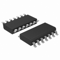
MC74HC164ADR2 ON Semiconductor, MC74HC164ADR2 Datasheet - Page 6

MC74HC164ADR2
Manufacturer Part Number
MC74HC164ADR2
Description
IC SHIFT REGISTER 8BIT 14SOIC
Manufacturer
ON Semiconductor
Series
74HCr
Datasheet
1.MC74HC164ADG.pdf
(11 pages)
Specifications of MC74HC164ADR2
Logic Type
Shift Register
Output Type
Standard
Number Of Elements
1
Number Of Bits Per Element
8
Function
Serial to Parallel
Voltage - Supply
2 V ~ 6 V
Operating Temperature
-55°C ~ 125°C
Mounting Type
Surface Mount
Package / Case
14-SOIC (3.9mm Width), 14-SOL
Lead Free Status / RoHS Status
Contains lead / RoHS non-compliant
Other names
MC74HC164ADR2OSCT
Available stocks
Company
Part Number
Manufacturer
Quantity
Price
Part Number:
MC74HC164ADR2
Manufacturer:
MOT/ON
Quantity:
20 000
Company:
Part Number:
MC74HC164ADR2G
Manufacturer:
ON
Quantity:
12 500
Part Number:
MC74HC164ADR2G
Manufacturer:
ON/安森美
Quantity:
20 000
INPUTS
A1, A2 (Pins 1, 2)
to be entered into the first stage of the shift register. For a
high level to be entered into the shift register, both A1 and
A2 inputs must be high, thereby allowing one input to be
used as a data−enable input. When only one serial input is
used, the other must be connected to V
Clock (Pin 8)
pin shifts the data at each stage to the next stage. The shift
Serial Data Inputs. Data at these inputs determine the data
Shift Register Clock. A positive−going transition on this
CLOCK
A1 OR A2
Q
CLOCK
10%
50%
90%
10%
50%
90%
t
r
t
w
t
PLH
t
TLH
50%
Figure 1.
Figure 3.
t
su
1/f
max
VALID
t
PHL
t
f
50%
t
THL
CC
t
h
.
SWITCHING WAVEFORMS
PIN DESCRIPTIONS
GND
V
CC
http://onsemi.com
V
GND
V
GND
CC
CC
6
register is completely static, allowing clock rates down to
DC in a continuous or intermittent mode.
OUTPUTS
Q
presented at these outputs in true, or noninverted, form.
CONTROL INPUT
Reset (Pin 9)
applied to this input resets all internal flip−flops and sets
Outputs Q
A
Parallel Shift Register Outputs. The shifted data is
Active−Low, Asynchronous Reset Input. A low voltage
CLOCK
RESET
− Q
Q
H
(Pins 3, 4, 5, 6, 10, 11, 12, 13)
A
− Q
*Includes all probe and jig capacitance
t
H
PHL
to the low level state.
DEVICE
UNDER
Figure 4. Test Circuit
TEST
50%
Figure 2.
t
w
t
50%
rec
OUTPUT
50%
TEST POINT
C
L
*
V
GND
GND
V
CC
CC


