CD4066BCM Fairchild Semiconductor, CD4066BCM Datasheet - Page 2
CD4066BCM
Manufacturer Part Number
CD4066BCM
Description
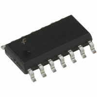
IC SWITCH BILATERAL QUAD 14-SOIC
Manufacturer
Fairchild Semiconductor
Series
4000Br
Type
Bilateral, FET Switchesr
Datasheet
1.CD4066BCM.pdf
(9 pages)
Specifications of CD4066BCM
Circuit
1 x 1:1
Independent Circuits
4
Voltage Supply Source
Dual Supply
Voltage - Supply
3 V ~ 15 V
Operating Temperature
-55°C ~ 125°C
Mounting Type
Surface Mount
Package / Case
14-SOIC (3.9mm Width), 14-SOL
Switch Configuration
SPST
On Resistance (max)
1050 Ohms
On Time (max)
125 ns
Off Time (max)
125 ns
Supply Voltage (max)
15 V
Supply Voltage (min)
3 V
Maximum Power Dissipation
500 mW
Maximum Operating Temperature
+ 125 C
Mounting Style
SMD/SMT
Minimum Operating Temperature
- 55 C
Propagation Delay Time
55 ns
Multiplexer Configuration
Quad SPST
Number Of Inputs
4
Number Of Outputs
4
Number Of Channels
4
Analog Switch On Resistance
1050@5VOhm
Analog Switch Turn On Time
125ns
Analog Switch Turn Off Time
125ns
Package Type
SOIC N
Power Supply Requirement
Single
Single Supply Voltage (min)
3V
Single Supply Voltage (typ)
5/9/12V
Single Supply Voltage (max)
15V
Dual Supply Voltage (min)
Not RequiredV
Dual Supply Voltage (typ)
Not RequiredV
Dual Supply Voltage (max)
Not RequiredV
Power Dissipation
500mW
Mounting
Surface Mount
Pin Count
14
Operating Temp Range
-55C to 125C
Operating Temperature Classification
Military
Dc
08+
Lead Free Status / RoHS Status
Lead free / RoHS Compliant
Current - Output High, Low
-
Lead Free Status / Rohs Status
Lead free / RoHS Compliant
Available stocks
Company
Part Number
Manufacturer
Quantity
Price

Part Number:
CD4066BCM
Manufacturer:
FAIRCHILD/ن»™ç«¥
Quantity:
20 000
Part Number:
CD4066BCMX
Manufacturer:
NS/ه›½هچٹ
Quantity:
20 000


www.fairchildsemi.com
I
SIGNAL INPUTS AND OUTPUTS
R
I
CONTROL INPUTS
V
V
I
Symbol
DD
IS
IN
Absolute Maximum Ratings
(Note 1)
(Note 2)
DC Electrical Characteristics
R
ILC
IHC
ON
ON
Supply Voltage (V
Input Voltage (V
Storage Temperature Range (T
Power Dissipation (P
Lead Temperature (T
Dual-In-Line
Small Outline
(Soldering, 10 seconds)
Quiescent Device Current
“ON” Resistance
Any 2 of 4 Switches
Input or Output Leakage
LOW Level Input
Voltage
HIGH Level Input
Voltage
Input Current
Switch “OFF”
“ON” Resistance Between
Parameter
IN
)
DD
)
D
L
)
)
S
)
V
V
V
R
V
V
V
V
R
V
V
V
V
V
V
I
V
V
V
V
V
V
V
V
V
IS
DD
DD
DD
C
DD
DD
DD
CC
DD
DD
C
IS
OS
DD
DD
DD
DD
DD
DD
DD
DD
DD
L
L
10 k to (V
10 k to (V
V
0
V
V
V
0.5V to V
V
5V
10V
15V
5V
10V
15V
V
10V
15V
V
10 A
5V
10V
15V
5V
10V (Note 7)
15V
DD
SS
IS
C
SS
65 C to 150 C
DD
DD
Conditions
, V
V
V
and V
0.5V to 18V
, V
SS
15V
and V
SS
SS
IS
to V
(Note 2)
CC
700 mW
500 mW
DD
DD
DD
SS
V
300 C
DD
SS
0.5V
V
V
to V
SS
SS
/2)
/2)
DD
2
Recommended Operating
Conditions
Note 1: “Absolute Maximum Ratings” are those values beyond which the
safety of the device cannot be guaranteed. They are not meant to imply
that the devices should be operated at these limits. The tables of “Recom-
mended Operating Conditions” and “Electrical Characteristics” provide con-
ditions for actual device operation.
Note 2: V
11.0
Supply Voltage (V
Input Voltage (V
Operating Temperature Range (T
Min
3.5
7.0
40 C
SS
Max
850
330
210
1.0
2.0
4.0
1.5
3.0
4.0
50
0.3
0V unless otherwise specified.
11.0
Min
3.5
7.0
IN
)
DD
(Note 2)
)
0.01
0.01
0.01
2.25
6.75
2.75
8.25
Typ
270
120
25 C
4.5
5.5
10
80
10
0.1
5
5
1050
Max
400
240
1.0
2.0
4.0
1.5
3.0
4.0
50
0.3
A
)
11.0
Min
3.5
7.0
85 C
40 C to 85 C
1200
Max
520
300
7.5
1.5
3.0
4.0
15
30
200
1.0
3V to 15V
0V to V
Units
DD
nA
V
V
V
V
V
V
A
A
A
A
Related parts for CD4066BCM
Image
Part Number
Description
Manufacturer
Datasheet
Request
R

Part Number:
Description:
Fairchild Semiconductor [IGBT MODULE]
Manufacturer:
Fairchild Semiconductor
Datasheet:

Part Number:
Description:
Discrete Semiconductor Modules
Manufacturer:
Fairchild Semiconductor
Part Number:
Description:
Discrete Semiconductor Modules
Manufacturer:
Fairchild Semiconductor
Part Number:
Description:
This N-Channel MOSFET is produced using Fairchild Semiconductor’s advanced Power Trench® process
Manufacturer:
Fairchild Semiconductor
Datasheet:
Part Number:
Description:
This N-Channel MOSFET is produced using Fairchild Semiconductor’s advanced Power Trench® process
Manufacturer:
Fairchild Semiconductor
Datasheet:
Part Number:
Description:
This N-Channel MOSFET is produced using Fairchild Semiconductor’s advanced PowerTrench® process
Manufacturer:
Fairchild Semiconductor
Datasheet:
Part Number:
Description:
This N-Channel MOSFET is produced using Fairchild Semiconductor’s advanced PowerTrench® process
Manufacturer:
Fairchild Semiconductor
Datasheet:
Part Number:
Description:
This N-Channel MOSFET is produced using Fairchild Semiconductor’s advanced Power Trench® process
Manufacturer:
Fairchild Semiconductor
Datasheet:
Part Number:
Description:
This N-Channel logic Level MOSFETs are produced using Fairchild Semiconductor‘s advanced Power Trench® process that has been special tailored to minimize the on-state resistance and yet maintain superior switching performance
Manufacturer:
Fairchild Semiconductor
Datasheet:
Part Number:
Description:
This N-Channel MOSFET is produced using Fairchild Semiconductor’s advanced Power Trench® process
Manufacturer:
Fairchild Semiconductor
Datasheet:
Part Number:
Description:
This N-Channel SyncFET™ is produced using Fairchild Semiconductor’s advanced PowerTrench® process
Manufacturer:
Fairchild Semiconductor
Datasheet:
Part Number:
Description:
This N-Channel SyncFET™ is produced using Fairchild Semiconductor’s advanced PowerTrench® process
Manufacturer:
Fairchild Semiconductor
Datasheet:
Part Number:
Description:
This N-Channel SyncFET™ is produced using Fairchild Semiconductor’s advanced PowerTrench® process
Manufacturer:
Fairchild Semiconductor
Datasheet:
Part Number:
Description:
This N-Channel logic Level MOSFETs are produced using Fairchild Semiconductor‘s advanced Power Trench® process that has been special tailored to minimize the on-state resistance and yet maintain superior switching performance
Manufacturer:
Fairchild Semiconductor
Datasheet:
Part Number:
Description:
This N-Channel MOSFET is produced using Fairchild Semiconductor’s advanced Power Trench® process that has been especially tailored to minimize the on-state resistance and yet maintain superior switching performance
Manufacturer:
Fairchild Semiconductor
Datasheet: