74ACT257SC Fairchild Semiconductor, 74ACT257SC Datasheet - Page 2
74ACT257SC
Manufacturer Part Number
74ACT257SC
Description
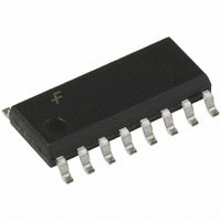
IC MUX QUAD 2-INPUT 3ST 16-SOIC
Manufacturer
Fairchild Semiconductor
Series
74ACTr
Type
Multiplexerr
Datasheet
1.74ACT257SC.pdf
(9 pages)
Specifications of 74ACT257SC
Circuit
4 x 2:1
Independent Circuits
1
Current - Output High, Low
24mA, 24mA
Voltage Supply Source
Single Supply
Voltage - Supply
4.5 V ~ 5.5 V
Operating Temperature
-40°C ~ 85°C
Mounting Type
Surface Mount
Package / Case
16-SOIC (3.9mm Width)
Logical Function
Mux
Configuration
4 x 2:1
Number Of Inputs
8
Number Of Outputs
4
Operating Supply Voltage (typ)
5V
Operating Supply Voltage (min)
4.5V
Operating Supply Voltage (max)
5.5V
Operating Temp Range
-40C to 85C
Operating Temperature Classification
Industrial
Mounting
Surface Mount
Pin Count
16
Package Type
SOIC N
Lead Free Status / RoHS Status
Lead free / RoHS Compliant
Available stocks
Company
Part Number
Manufacturer
Quantity
Price


www.fairchildsemi.com
Functional Description
The AC/ACT257 is quad 2-input multiplexer with 3-STATE
outputs. It selects four bits of data from two sources under
control of a Common Data Select input. When the Select
input is LOW, the I
is HIGH, the I
selected inputs appears at the outputs in true (noninverted)
form. The device is the logic implementation of a 4-pole, 2-
position switch where the position of the switch is deter-
mined by the logic levels supplied to the Select input. The
logic equations for the outputs are as follows:
When the Output Enable (OE) is HIGH, the outputs are
forced to a high impedance state. If the outputs are tied
together, all but one device must be in the high impedance
state to avoid high currents that would exceed the maxi-
mum ratings. Designers should ensure the Output Enable
signals to 3-STATE devices whose outputs are tied
together are designed so there is no overlap.
Logic Diagram
Please note that this diagram is provided only for the understanding of logic operations and should not be used to estimate propagation delays.
Z
Z
Z
Z
a
b
c
d
OE • (1
OE • (1
OE • (1
OE • (1
1x
1a
1b
1c
1d
inputs are selected. The data on the
0x
• S
• S
• S
• S
inputs are selected and when Select
I
I
I
I
0c
0a
0b
0d
• S)
• S)
• S)
• S)
2
Truth Table
H
L
X
Z
LOW Voltage Level
High Impedance
HIGH Voltage Level
Immaterial
Output
Enable
OE
H
L
L
L
L
Select
Input
S
X
H
H
L
L
I
X
X
X
H
L
0
Inputs
Data
I
X
H
X
X
L
1
Outputs
H
H
Z
Z
L
L
Related parts for 74ACT257SC
Image
Part Number
Description
Manufacturer
Datasheet
Request
R

Part Number:
Description:
IC BUFF/DVR TRI-ST DUAL 20SOIC
Manufacturer:
Fairchild Semiconductor
Datasheet:

Part Number:
Description:
IC BUFF TRI-ST QD N-INV 14SOIC
Manufacturer:
Fairchild Semiconductor
Datasheet:

Part Number:
Description:
IC BUFF/DVR TRI-ST 8BIT 20DIP
Manufacturer:
Fairchild Semiconductor
Datasheet:

Part Number:
Description:
IC BUFF/DVR TRI-ST DUAL 20TSSOP
Manufacturer:
Fairchild Semiconductor
Datasheet:
Part Number:
Description:
IC BUFF/DVR TRI-ST DUAL 20TSSOP
Manufacturer:
Fairchild Semiconductor
Datasheet:

Part Number:
Description:
IC F/F DUAL POS EDGE TRIG 14-DIP
Manufacturer:
Fairchild Semiconductor
Part Number:
Description:
IC F/F DUAL POS EDGE TRIG 14SOIC
Manufacturer:
Fairchild Semiconductor
Part Number:
Description:
IC FLIP FLOP OCTAL D 3ST 20TSSOP
Manufacturer:
Fairchild Semiconductor
Part Number:
Description:
IC FLIP FLOP OCTAL D 3ST 20-DIP
Manufacturer:
Fairchild Semiconductor

Part Number:
Description:
IC FLIP FLOP D TYPE QUAD 16SOIC
Manufacturer:
Fairchild Semiconductor
Datasheet:

Part Number:
Description:
IC FLIP FLOP OCT 20-TSSOP
Manufacturer:
ON Semiconductor
Datasheet:

Part Number:
Description:
IC FLIP FLOP OCT D 3ST 20-SOIC
Manufacturer:
ON Semiconductor
Datasheet:
Part Number:
Description:
IC INVERTER HEX 14-SOIC
Manufacturer:
Fairchild Semiconductor
Datasheet:
Part Number:
Description:
IC GATE OR QUAD 2-INPUT 14-SOIC
Manufacturer:
Fairchild Semiconductor
Datasheet:
Part Number:
Description:
IC INVERTER HEX SCHM TRIG 14SOIC
Manufacturer:
Fairchild Semiconductor
Datasheet: