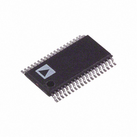
ADG3247BRU-REEL7 Analog Devices Inc, ADG3247BRU-REEL7 Datasheet - Page 3

ADG3247BRU-REEL7
Manufacturer Part Number
ADG3247BRU-REEL7
Description
IC SW BUS 2.5/3.3V 16BIT 38TSSOP
Manufacturer
Analog Devices Inc
Type
Bus Switchr
Datasheet
1.ADG3247BCPZ.pdf
(12 pages)
Specifications of ADG3247BRU-REEL7
Rohs Status
RoHS non-compliant
Circuit
8 x 1:1
Independent Circuits
2
Voltage Supply Source
Single Supply
Voltage - Supply
2.5V, 3.3V
Mounting Type
Surface Mount
Package / Case
38-TSSOP
Operating Temperature
-
Current - Output High, Low
-
ABSOLUTE MAXIMUM RATINGS*
(T
V
Digital Inputs to GND . . . . . . . . . . . . . . . . . –0.5 V to +4.6 V
DC Input Voltage . . . . . . . . . . . . . . . . . . . . . –0.5 V to +4.6 V
DC Output Current . . . . . . . . . . . . . . . . . . 25 mA per channel
Operating Temperature Range
Storage Temperature Range . . . . . . . . . . . . –65°C to +150°C
Junction Temperature . . . . . . . . . . . . . . . . . . . . . . . . . . 150°C
CAUTION
ESD (electrostatic discharge) sensitive device. Electrostatic charges as high as 4000 V readily
accumulate on the human body and test equipment and can discharge without detection. Although the
ADG3247 features proprietary ESD protection circuitry, permanent damage may occur on devices
subjected to high energy electrostatic discharges. Therefore, proper ESD precautions are recommended
to avoid performance degradation or loss of functionality.
REV. 0
Industrial (B Version) . . . . . . . . . . . . . . . . . –40°C to +85°C
CC
A
= 25°C, unless otherwise noted.)
to GND . . . . . . . . . . . . . . . . . . . . . . . . . –0.5 V to +4.6 V
Model
ADG3247BCP
ADG3247BCP-REEL7
ADG3247BRU
ADG3247BRU-REEL7
Mnemonic Description
BEx
SEL
Ax
Bx
A10
A11
A12
A13
A14
A15
A6
A7
A8
A9
10
2
3
4
5
6
7
8
9
1
Table I. Pin Description
NC = NO CONNECT
Bus Enable (Active Low)
Level Translation Select
Port A, Inputs or Outputs
Port B, Inputs or Outputs
PIN 1
INDICATOR
ADG3247
TOP VIEW
Temperature Range
–40°C to +85°C
–40°C to +85°C
–40°C to +85°C
–40°C to +85°C
30 B0
29 B1
28 B2
27 B3
26 B4
25 B5
24 B6
23 B7
22 B8
21 B9
40-Lead LFCSP and 38-Lead TSSOP
PIN CONFIGURATION
ORDERING GUIDE
Package Description
Lead Frame Chip Scale Package (LFCSP)
Lead Frame Chip Scale Package (LFCSP)
Thin Shrink Small Outline Package (TSSOP)
Thin Shrink Small Outline Package (TSSOP)
–3–
LFCSP Package
TSSOP Package
Lead Temperature, Soldering (10 seconds) . . . . . . . . . . 300°C
IR Reflow, Peak Temperature (<20 seconds) . . . . . . . . 235°C
*Stresses above those listed under Absolute Maximum Ratings may cause perma-
BEx SEL* Function
L
L
H
*SEL = 0 only when V
nent damage to the device. This is a stress rating only; functional operation of the
device at these or any other conditions above those listed in the opera tional
sections of this specification is not implied. Exposure to absolute maximum rating
conditions for extended periods may affect device reliability. Only one absolute
maximum rating may be applied at any one time.
θ
θ
JA
JA
Thermal Impedance . . . . . . . . . . . . . . . . . . . . . . . 32°C/W
Thermal Impedance . . . . . . . . . . . . . . . . . . . . . 98°C/W
L
H
X
A = B, 3.3 V to 1.8 V Level Shifting
A = B, 3.3 V to 2.5 V/2.5 V to 1.8 V Level Shifting
Disconnect
DD
= 3.3 V ± 10%
Table II. Truth Table
GND
SEL
A10
A11
A12
A13
A14
A15
NC = NO CONNECT
NC
A0
A1
A2
A3
A4
A5
A6
A7
A8
A9
10
11
12
13
14
15
16
17
18
19
1
2
3
4
5
6
7
8
9
ADG3247
(Not to Scale)
TOP VIEW
38
37
36
35
34
33
32
31
30
29
28
27
26
25
24
23
22
21
20
V
BE2
BE1
B0
B1
B2
B3
B4
B5
B6
B7
B8
B9
B10
B11
B12
B13
B14
B15
Package Option
CP-40
CP-40
RU-38
RU-38
CC
ADG3247


