N74F656AD,623 NXP Semiconductors, N74F656AD,623 Datasheet
N74F656AD,623
Specifications of N74F656AD,623
N74F656AD-T
N74F656AD-T


Related parts for N74F656AD,623


N74F656AD,623 Summary of contents
Page 1
Octal buffer/driver with parity; non-inverting; 3-state Rev. 05 — 25 March 2010 1. General description The 74F656A is an octal buffer and line driver with parity generation/checking. The 74F656A can be used as memory address driver, clock driver and ...
Page 2
... NXP Semiconductors 4. Functional diagram OE0 2 OE1 23 OE2 Fig 1. Logic symbol 74F656A_5 Product data sheet Octal buffer/driver with parity; non-inverting; 3-state ΣE 21 Σ 001aal255 Fig 2. Rev. 05 — 25 March 2010 74F656A [EVEN 10, 11 [ODD] 9, 10, 11 ≥1 2 EN4 Z10 10 Z11 11 Z12 IEC logic symbol © ...
Page 3
... NXP Semiconductors OE0 2 OE1 23 OE2 Fig 3. Logic diagram 74F656A_5 Product data sheet Octal buffer/driver with parity; non-inverting; 3-state Rev. 05 — 25 March 2010 74F656A 21 ΣE 22 Σ 001aal253 © NXP B.V. 2010. All rights reserved ...
Page 4
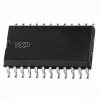
... NXP Semiconductors 5. Pinning information 5.1 Pinning Fig 4. Pin configuration 5.2 Pin description Table 2. Pin description Symbol Pin OE0 1 OE1 10, 11 GND 20, 19, 18, 17, 16, 15, 14, 13 ΣE 21 ΣO 22 OE2 One FAST Unit Load (UL) is defined as 20 μ [1] 74F656A_5 Product data sheet Octal buffer/driver with parity; non-inverting; 3-state ...
Page 5
... NXP Semiconductors 6. Functional description 6.1 Function table [1] Table 3. Function selection Input OE0 OE1 [ HIGH voltage level LOW voltage level don’t care high-impedance OFF-state. Table 4. Function parity outputs Inputs State Even number of inputs H ( Odd number of inputs H ( Any OEn H [ HIGH voltage level; ...
Page 6
... NXP Semiconductors 7. Limiting values Table 5. Limiting values In accordance with the Absolute Maximum Rating System (IEC 60134). Symbol Parameter V supply voltage CC V input voltage I V output voltage O I input clamping current IK I output current O T ambient temperature amb T storage temperature stg [1] The input and output voltage ratings may be exceeded if the input and output current ratings are observed. ...
Page 7
... NXP Semiconductors Table 7. Static characteristics Symbol Parameter V LOW-level output OL voltage I input leakage current I I HIGH-level input current LOW-level input current IL I OFF-state output current output current O I supply current CC [1] All typical values are measured at V [2] Not more than one output should be tested at a time, and the duration of the test should not exceed one second. ...
Page 8
... NXP Semiconductors Table 8. Dynamic characteristics GND = 0 V; for test circuit, see Figure Symbol Parameter Conditions t OFF-state to LOW OEn to Qn; PZL propagation delay see t HIGH to OFF-state OEn to Qn; PHZ propagation delay see t LOW to OFF-state OEn to Qn; PLZ propagation delay see 11. Waveforms Propagation delay input Dn to output Qn, Σ ...
Page 9
... NXP Semiconductors negative V M pulse positive V M pulse Input pulse definition Test data and V levels are given in EXT R = Load resistance Load capacitance including jig and probe capacitance Termination resistance should be equal to output impedance Test voltage for switching times. EXT Fig 7. Test circuit for measuring switching times Table 9 ...
Page 10
... NXP Semiconductors 12. Package outline SO24: plastic small outline package; 24 leads; body width 7 pin 1 index 1 e DIMENSIONS (inch dimensions are derived from the original mm dimensions) A UNIT max. 0.3 2.45 mm 2.65 0.25 0.1 2.25 0.012 0.096 inches 0.1 0.01 0.004 0.089 Note 1. Plastic or metal protrusions of 0.15 mm (0.006 inch) maximum per side are not included. ...
Page 11
... Modifications: The format of this data sheet has been redesigned to comply with the new identity guidelines of NXP Semiconductors. • Legal texts have been adapted to the new company name where appropriate. • DIP 24 (SOT222-1) package removed from 12 “Package outline” ...
Page 12
... In no event shall NXP Semiconductors be liable for any indirect, incidental, punitive, special or consequential damages (including - without limitation - lost profits, lost savings, business interruption, costs related to the removal or ...
Page 13
... NXP Semiconductors 16. Contact information For more information, please visit: For sales office addresses, please send an email to: 74F656A_5 Product data sheet Octal buffer/driver with parity; non-inverting; 3-state http://www.nxp.com salesaddresses@nxp.com Rev. 05 — 25 March 2010 74F656A © NXP B.V. 2010. All rights reserved. ...
Page 14
... NXP Semiconductors 17. Contents 1 General description . . . . . . . . . . . . . . . . . . . . . . 1 2 Features . . . . . . . . . . . . . . . . . . . . . . . . . . . . . . . 1 3 Ordering information . . . . . . . . . . . . . . . . . . . . . 1 4 Functional diagram . . . . . . . . . . . . . . . . . . . . . . 2 5 Pinning information . . . . . . . . . . . . . . . . . . . . . . 4 5.1 Pinning . . . . . . . . . . . . . . . . . . . . . . . . . . . . . . . 4 5.2 Pin description . . . . . . . . . . . . . . . . . . . . . . . . . 4 6 Functional description . . . . . . . . . . . . . . . . . . . 5 6.1 Function table . . . . . . . . . . . . . . . . . . . . . . . . . . 5 7 Limiting values Recommended operating conditions Static characteristics Dynamic characteristics . . . . . . . . . . . . . . . . . . 7 11 Waveforms . . . . . . . . . . . . . . . . . . . . . . . . . . . . . 8 12 Package outline . . . . . . . . . . . . . . . . . . . . . . . . 10 13 Abbreviations ...