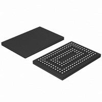
SSTUH32865ET/G,518 NXP Semiconductors, SSTUH32865ET/G,518 Datasheet - Page 6

SSTUH32865ET/G,518
Manufacturer Part Number
SSTUH32865ET/G,518
Description
IC BUFFER 1.8V 28BIT SOT802-1
Manufacturer
NXP Semiconductors
Datasheet
1.SSTUH32865ETG551.pdf
(28 pages)
Specifications of SSTUH32865ET/G,518
Logic Type
1:2 Registered Buffer with Parity
Supply Voltage
1.7 V ~ 1.9 V
Number Of Bits
28
Operating Temperature
0°C ~ 70°C
Mounting Type
Surface Mount
Package / Case
160-TFBGA
Lead Free Status / RoHS Status
Lead free / RoHS Compliant
Other names
935277963518
SSTUH32865ET/G-T
SSTUH32865ET/G-T
SSTUH32865ET/G-T
SSTUH32865ET/G-T
Philips Semiconductors
Table 2:
9397 750 14136
Product data sheet
Symbol
Ungated inputs
DCKE0, DCKE1
DODT0, DODT1
Chip Select gated inputs
D0 to D21
Chip Select inputs
DCS0, DCS1
Re-driven outputs
Q0A to Q21A
Q0B to Q21B
QCS0A, QDS1A,
QCS0B, QCS1B
QCKE0A, QCKE1A,
QCKE0B, QCKE1B
QODT0A, QODT1A,
QODT0B, QODT1B
Parity input
PARIN
Parity error
PTYERR
Program inputs
CSGATEEN
Pin description
6.2 Pin description
Pin
U1, U2
T2, T1
M1, B1, B2, C1, C2, D2, D1,
E1, E2, F2, M2, F1, G2, R1,
L2, H2, N2, N1, G1, P1, R2,
P2
J2, K2
V11, F12, G12, V6, V9, H12,
L12, V8, V12, N12, M12,
P12, V7, V10, T12, R12,
E12, A12, A10, A9, D12, A8
U11, F11, G11, U6, U9,
H11, L11, U8, U12, N11,
M11, P11, U7, U10, T11,
R11, E11, A11, B10, B9,
D11, B8
J12, K12, J11, K11
A7, A6, B7, B6
B12, C12, B11, C11
A3
U4
H1
Rev. 01 — 11 March 2005
Type
SSTL_18
SSTL_18
SSTL_18
SSTL_18
SSTL_18
open drain
1.8 V
LVCMOS
1.8 V high output drive DDR registered buffer with parity
Description
DRAM function pins not associated with Chip Select.
DRAM inputs, re-driven only when Chip Select is LOW.
DRAM Chip Select signals. These pins initiate DRAM
address/command decodes, and as such at least one will
be LOW when a valid address/command is present. The
register can be programmed to re-drive all D-inputs only
(CSGATEEN = HIGH) when at least one Chip Select
input is LOW.
Outputs of the register, valid after the specified clock
count and immediately following a rising edge of the
clock.
Parity input for the D0 to D21 inputs. Arrives one clock
cycle after the corresponding data input.
When LOW, this output indicates that a parity error was
identified associated with the address and/or command
inputs. PTYERR will be active for two clock cycles, and
delayed by an additional clock cycle for compatibility with
final parity out timing on the industry-standard DDR2
register with parity (in JEDEC definition).
Chip Select Gate Enable. When HIGH, the D0 to D21
inputs will be latched only when at least one Chip Select
input is LOW during the rising edge of the clock. When
LOW, the D0 to D21 inputs will be latched and redriven
on every rising edge of the clock.
© Koninklijke Philips Electronics N.V. 2005. All rights reserved.
SSTUH32865
6 of 28


