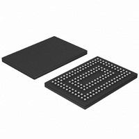
SSTUG32865ET/G,518 NXP Semiconductors, SSTUG32865ET/G,518 Datasheet - Page 17

SSTUG32865ET/G,518
Manufacturer Part Number
SSTUG32865ET/G,518
Description
IC BUFFER 1.8V 28BIT 160-TFBGA
Manufacturer
NXP Semiconductors
Datasheet
1.SSTUG32865ETG518.pdf
(28 pages)
Specifications of SSTUG32865ET/G,518
Logic Type
1:2 Registered Buffer with Parity
Supply Voltage
1.7 V ~ 2 V
Number Of Bits
28
Operating Temperature
0°C ~ 70°C
Mounting Type
Surface Mount
Package / Case
160-TFBGA
Lead Free Status / RoHS Status
Lead free / RoHS Compliant
Other names
935284903518
SSTUG32865ET/G-T
SSTUG32865ET/G-T
SSTUG32865ET/G-T
SSTUG32865ET/G-T
Available stocks
Company
Part Number
Manufacturer
Quantity
Price
Company:
Part Number:
SSTUG32865ET/G,518
Manufacturer:
NXP Semiconductors
Quantity:
10 000
NXP Semiconductors
Table 11.
Over recommended operating conditions, unless otherwise noted.
[1]
[2]
[3]
Table 12.
Over recommended operating conditions, unless otherwise noted.
[1]
[2]
Table 13.
Over recommended operating conditions, unless otherwise noted.
SSTUG32865_1
Product data sheet
Symbol
f
t
t
t
t
t
Symbol
f
t
t
t
t
t
t
Symbol
dV/dt_r
dV/dt_f
dV/dt_
clock
W
ACT
INACT
su
h
max
PDM
LH
HL
PLH
PDMSS
PHL
This parameter is not necessarily production tested.
Data inputs must be active below a minimum time of t
Data and clock inputs must be held at valid levels (not floating) a minimum time of t
Includes 350 ps of test-load transmission line delay.
This parameter is not necessarily production tested.
Timing requirements
Switching characteristics
Output edge rates
Parameter
clock frequency
pulse width
differential inputs active time
differential inputs inactive time
set-up time
hold time
Parameter
maximum input clock frequency
peak propagation delay
LOW to HIGH delay time
HIGH to LOW delay time
LOW-to-HIGH propagation delay
simultaneous switching peak
propagation delay
HIGH-to-LOW propagation delay
Parameter
rising edge slew rate
falling edge slew rate
absolute difference between dV/dt_r
and dV/dt_f
Rev. 01 — 16 August 2007
Conditions
CK, CK HIGH or LOW
Chip Select; DCS0, DCS1
valid before clock
switching
Data; Dn valid before
clock switching
PARIN; PARIN before CK
and CK
input to remain valid after
clock switching
PARIN after CK and CK
Conditions
CK and CK to output
CK and CK to PTYERR
CK and CK to PTYERR
from RESET to PTYERR
CK and CK to output
RESET to output
Conditions
ACT(max)
after RESET is taken HIGH.
1.8 V DDR2-1G registered buffer with parity
INACT(max)
[1][2]
[1][3]
[1][2]
[1]
after RESET is taken LOW.
Min
-
1
-
-
0.6
0.5
0.5
0.4
0.4
Min
550
1.0
1.2
1
-
-
-
Min
1
1
-
SSTUG32865
Typ
-
-
-
-
-
-
-
-
-
Typ
-
-
-
-
-
-
-
Typ
-
-
-
© NXP B.V. 2007. All rights reserved.
Max
550
-
10
15
-
-
-
-
-
Max
-
1.4
3
3
3
1.5
3
Max
4
4
1
Unit
MHz
ns
ns
ns
ns
ns
ns
ns
ns
Unit
MHz
ns
ns
ns
ns
ns
ns
Unit
V/ns
V/ns
V/ns
17 of 28


