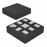
PCA9306GM,125 NXP Semiconductors, PCA9306GM,125 Datasheet - Page 6

PCA9306GM,125
Manufacturer Part Number
PCA9306GM,125
Description
IC LEVEL TRANSLATOR 8-XQFN
Manufacturer
NXP Semiconductors
Datasheet
1.PCA9306DP118.pdf
(26 pages)
Specifications of PCA9306GM,125
Package / Case
8-XQFN
Logic Function
Translator, Bidirectional, Open Drain
Number Of Bits
2
Input Type
Voltage
Output Type
Voltage
Number Of Channels
2
Number Of Outputs/channel
1
Differential - Input:output
No/No
Voltage - Supply
1 V ~ 3.6 V, 1.8 V ~ 5.5 V
Operating Temperature
-40°C ~ 85°C
Supply Voltage
1.2 V ~ 5.5 V
Logic Family
PCA
Supply Voltage (max)
5 V
Supply Voltage (min)
1 V
Maximum Operating Temperature
+ 85 C
Minimum Operating Temperature
- 40 C
Interface Type
I2C
Mounting Style
SMD/SMT
Lead Free Status / RoHS Status
Lead free / RoHS Compliant
Data Rate
-
Lead Free Status / Rohs Status
Lead free / RoHS Compliant
Other names
568-4187-2
935283123125
PCA9306GM-G
935283123125
PCA9306GM-G
NXP Semiconductors
6. Functional description
7. Limiting values
8. Recommended operating conditions
PCA9306
Product data sheet
6.1 Function table
Refer to
Table 3.
H = HIGH level; L = LOW level.
[1]
Table 4.
In accordance with the Absolute Maximum Rating System (IEC 60134).
Over operating free-air temperature range.
[1]
Table 5.
[1]
Input EN
H
L
Symbol
V
V
V
V
I
I
T
Symbol
V
V
V
V
I
T
ch
IK
sw(pass)
stg
amb
ref(1)
bias(ref)(2)
I
I/O
I/O
ref(1)
bias(ref)(2)
I(EN)
EN is controlled by the V
translator operation.
The input and input/output negative voltage ratings may be exceeded if the input and input/output clamp
current ratings are observed.
V
ref(1)
[1]
Figure 1 “Logic diagram of PCA9306 (positive
[1]
≤ V
[1]
Function selection (example)
Limiting values
Operating conditions
Parameter
reference voltage (1)
reference bias voltage (2)
input voltage
voltage on an input/output pin
channel current (DC)
input clamping current
storage temperature
bias(ref)(2)
Parameter
voltage on an input/output pin SCL1, SDA1,
reference voltage (1)
reference bias voltage (2)
input voltage on pin EN
pass switch current
ambient temperature
Function
SCL1 = SCL2; SDA1 = SDA2
disconnect
All information provided in this document is subject to legal disclaimers.
− 1 V for best results in level shifting applications.
Rev. 6 — 25 November 2010
Dual bidirectional I
bias(ref)(2)
logic levels and should be at least 1 V higher than V
VREF1
operating in free-air
Conditions
SCL2, SDA2
VREF2
Conditions
V
I
2
< 0 V
C-bus and SMBus voltage-level translator
logic)”.
Min
−0.5
−0.5
−0.5
−0.5
-
-
−65
[1]
[1]
Min
0
0
0
0
-
−40
PCA9306
© NXP B.V. 2010. All rights reserved.
Max
+6
+6
+6
+6
128
−50
+150
ref(1)
Max
5
5
5
5
64
+85
for best
Unit
V
V
V
V
mA
°C
Unit
V
V
V
V
mA
mA
°C
6 of 26


