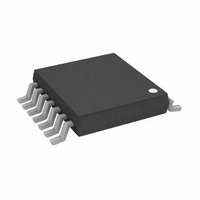
ADG3304BRUZ Analog Devices Inc, ADG3304BRUZ Datasheet - Page 7

ADG3304BRUZ
Manufacturer Part Number
ADG3304BRUZ
Description
IC XLATOR 4CH 1.2/5.5V 14-TSSOP
Manufacturer
Analog Devices Inc
Datasheet
1.ADG3304BRUZ.pdf
(20 pages)
Specifications of ADG3304BRUZ
Logic Function
Translator, Bidirectional
Number Of Bits
4
Input Type
Logic
Output Type
Logic
Data Rate
50Mbps
Number Of Channels
4
Number Of Outputs/channel
1
Differential - Input:output
No/No
Propagation Delay (max)
6ns
Voltage - Supply
1.15 V ~ 5.5 V
Operating Temperature
-40°C ~ 85°C
Package / Case
14-TSSOP
Supply Voltage
1.5 V ~ 5.5 V
No. Of Inputs
4
Propagation Delay
6ns
Logic Type
Level Translator
Supply Voltage Range
1.15V To 5.5V
Logic Case Style
TSSOP
No. Of Pins
14
Operating Temperature Range
-40°C To +85°C
Lead Free Status / RoHS Status
Lead free / RoHS Compliant
Available stocks
Company
Part Number
Manufacturer
Quantity
Price
Company:
Part Number:
ADG3304BRUZ
Manufacturer:
ADI
Quantity:
3 000
Part Number:
ADG3304BRUZ
Manufacturer:
ADI/亚德诺
Quantity:
20 000
PIN CONFIGURATIONS AND FUNCTION DESCRIPTIONS
Table 3. 14-Lead TSSOP and 20-lead LFCSP Pin Function Descriptions
TSSOP
1
2
3
4
5
6, 9
7
8
10
11
12
13
14
Table 4. 12-Ball WLCSP Pin Function Descriptions
Bump No.
a1
a2
a3
a4
b1
b2
b3
b4
c1
c2
c3
c4
V
GND
CCA
NC
A1
A2
A3
A4
1
2
3
4
5
6
7
NC = NO CONNECT
Figure 2. 14-Lead TSSOP
(Not to Scale)
Pin Configuration
ADG3304
TOP VIEW
Mnemonic
Y1
Y2
Y3
Y4
V
V
EN
GND
A1
A2
A3
A4
CCY
CCA
Pin No.
LFCSP
19
20
2
3
4
1, 5, 6, 7, 10, 11, 15, 16
8
9
12
13
14
17
18
13
12
11
10
14
9
8
V
Y1
Y2
Y3
Y4
NC
EN
Description
Input/Output Y1. Referenced to V
Input/Output Y2. Referenced to V
Input/Output Y3. Referenced to V
Input/Output Y4. Referenced to V
Power Supply Voltage Input for the Y1 to Y4 I/O Pins (1.65 V ≤ V
Power Supply Voltage Input for the A1 to A4 I/O Pins (1.15 V ≤ V
Active High Enable Input.
Ground.
Input/Output A1. Referenced to V
Input/Output A2. Referenced to V
Input/Output A3. Referenced to V
Input/Output A4. Referenced to V
CCY
Mnemonic
V
A1
A2
A3
A4
NC
GND
EN
Y4
Y3
Y2
Y1
V
CCA
CCY
1
4
2
3
(BALLS AT THE BOTTOM)
Figure 3. 12-Ball WLCSP
BALL a1
INDICATOR
Pin Configuration
Y2
Y3
Y1
Y4
Rev. B | Page 7 of 20
a
Not to Scale
Description
Power Supply Voltage Input for the A1 to A4 I/O Pins (1.15 V ≤ V
Input/Output A1. Referenced to V
Input/Output A2. Referenced to V
Input/Output A3. Referenced to V
Input/Output A4. Referenced to V
No Connect.
Ground.
Active High Enable Input.
Input/Output Y4. Referenced to V
Input/Output Y3. Referenced to V
Input/Output Y2. Referenced to V
Input/Output Y1. Referenced to V
Power Supply Voltage Input for the Y1 to Y4 I/O Pins (1.65 V ≤ V
TOP VIEW
V
V
GND
CCY
CCY
CCY
CCY
CCA
CCA
CCA
CCA
EN
CCA
CCY
b
.
.
.
.
.
.
.
.
A1
A3
A4
A2
c
NOTES
1. THE EXPOSED PADDLE CAN BE TIED TO GND
OR LEFT FLOATING. DO NOT TIE IT TO V
CC
CCA
CCY
CCY
CCY
CCY
CCA
CCA
CCA
CCA
≤ 5.5 V).
≤ V
.
.
.
.
NC
NC
.
.
.
.
A2
A3
A4
CCY
1
2
3
4
5
).
Figure 4. 20-Lead LFCSP_VQ
NC = NO CONNECT
(Not to Scale)
ADG3304
TOP VIEW
Pin Configuration
PIN 1
INDICATOR
15 NC
14 Y2
13 Y3
12 Y4
11 NC
ADG3304
CC
CCA
CCA
≤ 5.5 V).
or V
≤ V
CCY.
CCY
).


