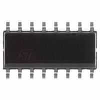
M74HC4050RM13TR STMicroelectronics, M74HC4050RM13TR Datasheet - Page 2

M74HC4050RM13TR
Manufacturer Part Number
M74HC4050RM13TR
Description
IC BUFF/CNVRTR HEX N-INV 16SOICN
Manufacturer
STMicroelectronics
Series
74HCr
Datasheet
1.M74HC4050TTR.pdf
(8 pages)
Specifications of M74HC4050RM13TR
Logic Type
Buffer/Line Driver, Non-Inverting
Number Of Elements
6
Number Of Bits Per Element
1
Current - Output High, Low
5.2mA, 5.2mA
Voltage - Supply
2 V ~ 6 V
Operating Temperature
-55°C ~ 125°C
Mounting Type
Surface Mount
Package / Case
16-SOIC (0.300", 7.5mm Width)
Supply Voltage
*
Output Type
*
Input Type
*
Number Of Channels
*
Data Rate
*
Logic Family
HC
Number Of Channels Per Chip
5
Polarity
Non-Inverting
Supply Voltage (max)
6 V
Supply Voltage (min)
2 V
Maximum Operating Temperature
+ 125 C
Mounting Style
SMD/SMT
High Level Output Current
- 5.2 mA
Low Level Output Current
5.2 mA
Maximum Power Dissipation
500 mW
Minimum Operating Temperature
- 55 C
Number Of Lines (input / Output)
6 / 3
Propagation Delay Time
100 ns at 2 V, 20 ns at 4.5 V, 17 ns at 6 V
Logic Device Type
Buffer, Non Inverting
Supply Voltage Range
2V To 6V
Logic Case Style
SOP
No. Of Pins
16
Operating Temperature Range
-55°C To +125°C
Filter Terminals
SMD
Rohs Compliant
Yes
Family Type
4000 CMOS
Lead Free Status / RoHS Status
Lead free / RoHS Compliant
Other names
497-1844-2
Available stocks
Company
Part Number
Manufacturer
Quantity
Price
Part Number:
M74HC4050RM13TR
Manufacturer:
ST
Quantity:
20 000
M74HC4050
INPUT AND OUTPUT EQUIVALENT CIRCUIT
ABSOLUTE MAXIMUM RATINGS
Absolute Maximum Ratings are those values beyond which damage to the device may occur. Functional operation under these conditions is
not implied
(*) 500mW at 65 C; derate to 300mW by 10mW/ C from 65 C to 85 C
RECOMMENDED OPERATING CONDITIONS
2/8
I
CC
Symbol
Symbol
V
V
T
t
I
or I
T
V
P
V
I
T
r
V
OK
I
V
stg
, t
CC
IK
O
CC
op
O
D
O
L
I
I
f
GND
Supply Voltage
DC Input Voltage
DC Output Voltage
DC Input Diode Current
DC Output Diode Current
DC Output Current
DC V
Power Dissipation
Storage Temperature
Lead Temperature (10 sec)
Supply Voltage
Input Voltage
Output Voltage
Operating Temperature
Input Rise and Fall Time
CC
or Ground Current
Parameter
Parameter
PIN DESCRIPTION
TRUTH TABLE
3, 5, 7, 9, 11,
2, 4, 6, 10,
V
V
V
PIN No
CC
CC
CC
12, 15
13, 16
14
8
1
= 2.0V
= 4.5V
= 6.0V
INPUT
nA
H
L
SYMBOL
1Y to 6Y
1A to 6A
GND
V
NC
CC
-0.5 to V
-65 to +150
-55 to 125
-0.5 to +7
-0.5 to 15
0 to 1000
0 to V
0 to 500
0 to 400
0 to 13
500(*)
Value
Value
2 to 6
Data Outputs
Data Inputs
Not Connected
Ground (0V)
Positive Supply Voltage
300
NAME AND FUNCTION
20
20
25
50
CC
CC
+ 0.5
OUTPUT
nY
H
L
Unit
Unit
mW
mA
mA
mA
mA
°C
°C
°C
ns
ns
ns
V
V
V
V
V
V


