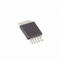
MAX9376EUB+ Maxim Integrated Products, MAX9376EUB+ Datasheet - Page 5

MAX9376EUB+
Manufacturer Part Number
MAX9376EUB+
Description
IC TRANSLATOR DUAL 10-UMAX
Manufacturer
Maxim Integrated Products
Datasheet
1.MAX9376EUB.pdf
(8 pages)
Specifications of MAX9376EUB+
Logic Function
Translator
Number Of Bits
2
Input Type
AnyLevel™
Output Type
LVDS, LVPECL
Number Of Channels
2
Number Of Outputs/channel
2
Differential - Input:output
Yes/No
Voltage - Supply
3 V ~ 3.6 V
Operating Temperature
-40°C ~ 85°C
Package / Case
10-MSOP, Micro10™, 10-uMAX, 10-uSOP
Supply Voltage
3 V ~ 3.6 V
Logic Type
Level Translator
Translation
LVDS to LVDS/LVPECL
Propagation Delay Time
0.6 ns
Supply Voltage (max)
3.6 V
Supply Voltage (min)
3 V
Maximum Operating Temperature
+ 85 C
Minimum Operating Temperature
- 40 C
Mounting Style
SMD/SMT
Lead Free Status / RoHS Status
Lead free / RoHS Compliant
Data Rate
-
Lead Free Status / Rohs Status
Lead free / RoHS Compliant
LVDS/Anything-to-LVPECL/LVDS Dual Translator
The MAX9376 is a fully differential, high-speed,
LVDS/anything-to-LVPECL/LVDS dual translator
designed for signal rates up to 2GHz. One channel is
LVDS/anything-to-LVPECL translator and the other
channel is LVDS/anything-to-LVDS translator. The
MAX9376’s extremely low propagation delay and high
speed make it ideal for various high-speed network
routing and backplane applications.
The MAX9376 accepts any differential input signal with-
in the supply rails and with a minimum amplitude of
100mV. Inputs are fully compatible with the LVDS,
LVPECL, HSTL, and CML differential signaling stan-
dards. LVPECL outputs have sufficient current to drive
50Ω transmission lines. LVDS outputs conform to the
ANSI EIA/TIA-644 LVDS standard.
Inputs have a wide common-mode range of 0.05V to
V
nals within rails, and requires a minimum of 100mV to
CC
- 0.05V, which accommodates any differential sig-
PIN
10
1
2
3
4
5
6
7
8
9
_______________________________________________________________________________________
NAME
OUT2
OUT2
OUT1
OUT1
GND
V
IN1
IN1
IN2
IN2
Detailed Description
CC
Differential LVDS/Anything Noninverting Input 1
Differential LVDS/Anything Inverting Input 1
Differential LVDS Noninverting Output 2. Terminate with 100Ω ±1% to OUT2.
Differential LVDS Inverting Output 2. Terminate with 100Ω ±1% to OUT2.
Ground
Differential LVDS/Anything Inverting Input 2
Differential LVDS/Anything Noninverting Input 2
Differential LVPECL Inverting Output. Terminate with 50Ω ±1% to V
Differential LVPECL Noninverting Output. Terminate with 50Ω ±1% to V
Positive Supply. Bypass from V
the capacitors as close to the device as possible with the smaller value capacitor closest to
the device.
Inputs
CC
switch the outputs. This allows the MAX9376 inputs to
support virtually any differential signaling standard.
The MAX9376 LVPECL outputs are emitter followers
that require external resistive paths to a voltage source
(V
V
properly terminated, the outputs generate steady-state
voltage levels, V
between state levels. Output current always flows into
the termination during proper operation.
The MAX9376 LVDS outputs require a resistive load to
terminate the signal and complete the transmission
loop. Because the device switches current and not volt-
age, the actual output voltage swing is determined by
the value of the termination resistor. With a 3.5mA typi-
cal output current, the MAX9376 produces an output
voltage of 350mV when driving a 100Ω load.
OL
T
to GND with 0.1µF and 0.01µF ceramic capacitors. Place
= V
for proper static and dynamic operation. When
CC
FUNCTION
- 2.0V typ) more negative than worst-case
OL
or V
OH
with fast transition edges
CC
Pin Description
- 2V.
LVPECL Outputs
CC
- 2V.
LVDS Outputs
5


