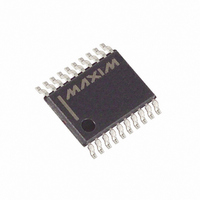
MAX3013EUP+ Maxim Integrated Products, MAX3013EUP+ Datasheet - Page 11

MAX3013EUP+
Manufacturer Part Number
MAX3013EUP+
Description
IC TRANSLATOR LEVEL 8CH 20TSSOP
Manufacturer
Maxim Integrated Products
Datasheet
1.MAX3013EUP.pdf
(17 pages)
Specifications of MAX3013EUP+
Logic Function
Translator, Bidirectional, 3-State
Number Of Bits
8
Input Type
Voltage
Output Type
Voltage
Data Rate
100Mbps
Number Of Channels
8
Number Of Outputs/channel
1
Differential - Input:output
No/No
Propagation Delay (max)
6ns
Voltage - Supply
1.65 V ~ 3.6 V
Operating Temperature
-40°C ~ 85°C
Package / Case
20-TSSOP
Supply Voltage
1.65 V ~ 3.6 V
Lead Free Status / RoHS Status
Lead free / RoHS Compliant
The MAX3013 logic-level translator provides the level
shifting necessary to allow 100Mbps data transfer in a
multivoltage system. Externally applied voltages, V
and V
Logic signals present on the V
appear as a higher voltage logic signal on the V
of the device, and vice-versa. The MAX3013 bidirection-
al level translator allows data translation in either direc-
tion (V
accepts V
V
fer between low-voltage ASICs/PLDs and higher voltage
systems.
The MAX3013 features an input enable mode (EN) that
reduces V
tristate mode. This device operates at a guaranteed
data rate of 100Mbps for V
For proper operation, ensure that +1.65V ≤ V
+1.2V ≤ V
V
supply sequencing, when V
ering up, up to 40mA current can be sourced to each
load on the V
The maximum data rate depends heavily on the load
capacitance (see the Typical Operating Characteristics,
Rise/Fall Times), output impedance of the driver, and the
operating voltage range (see the Timing Characteristics).
The MAX3013 architecture is based on a one-shot
accelerator output stage (see Figure 5). Accelerator
output stages are always in tristate mode except when
there is a transition on any of the translators on the
input side, either I/O V
is generated during which the accelerator output
stages become active and charge/discharge the
capacitances at the I/Os. Due to its bidirectional nature,
both input stages become active during the one-shot
pulse. This can lead to some current feeding into the
external source that is driving the translator. However,
this behavior helps to speed up the transition on the
driven side.
For proper operation, the external driver must meet the
following conditions: <25Ω output impedance and
>20mA output current. Figure 6 shows a graph of
Typical Input Current vs. Input Voltage.
CC
L
≥ V
from +1.65V to +3.6V, making it ideal for data trans-
L
L
CC
, set the logic levels on either side of the device.
↔ V
L
L
CC
does not damage the device. During power-
≤ (V
from +1.2V to (V
CC
and V
L
CC
) on any single data line. The MAX3013
side, yet the device does not latch up.
______________________________________________________________________________________
- 0.4V). During power-up sequencing,
L
supply currents to 0.1µA, when in
Input Driver Requirements
Detailed Description
L
or I/O V
L
CC
CC
> +1.8V.
is floating and V
- 0.4V) and operate with
CC
Level Translation
L
. Then, a short pulse
side of the device
+1.2V to +3.6V, 0.1µA, 100Mbps,
CC
L
≤ +3.6V,
CC
8-Channel Level Translators
is pow-
side
CC
The MAX3013 I/O was designed to drive CMOS inputs.
Do not load the I/O lines with a resistive load less than
25kΩ. Also, do not place an RC circuit at the input of
the MAX3013 to slow down the edges. If a slower data
rate is required, please see the MAX3000E/MAX3001E
logic-level translator.
For I
MAX3379E/MAX3390E–MAX3393E data sheet.
Figure 5. MAX3013 Simplified Diagram (1 I/O line)
IV
V
V
OV
2
L
L
L
C level translation, please refer to the MAX3372E–
L
150Ω
TYPICAL DRIVING ONE-CHANNEL ON V
TYPICAL DRIVING ONE-CHANNEL ON V
Output Load Requirements
150Ω
ONE-SHOT
ONE-SHOT
ONE-SHOT
P
N
ONE-SHOT
P
N
4kΩ
CC
L
SIDE
SIDE
4kΩ
OV
IV
V
V
CC
CC
CC
CC
11


