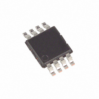
MAX9372EUA+ Maxim Integrated Products, MAX9372EUA+ Datasheet - Page 3

MAX9372EUA+
Manufacturer Part Number
MAX9372EUA+
Description
IC TRANSLATOR 8-UMAX
Manufacturer
Maxim Integrated Products
Datasheet
1.MAX9372EUA.pdf
(9 pages)
Specifications of MAX9372EUA+
Logic Function
Translator
Number Of Bits
2
Input Type
LVTTL, TTL
Output Type
LVPECL, PECL
Number Of Channels
2
Number Of Outputs/channel
1
Differential - Input:output
No/Yes
Propagation Delay (max)
0.27ns
Voltage - Supply
3 V ~ 3.6 V
Operating Temperature
-40°C ~ 85°C
Package / Case
8-MSOP, Micro8™, 8-uMAX, 8-uSOP,
Supply Voltage
3 V ~ 3.6 V
Lead Free Status / RoHS Status
Lead free / RoHS Compliant
Data Rate
-
DC ELECTRICAL CHARACTERISTICS (continued)
(V
Typical values are at V
AC ELECTRICAL CHARACTERISTICS
(V
frequency
2.4V, V
Note 1: Measurements are made with the device in thermal equilibrium.
Note 2: Current into a pin is defined as positive. Current out of a pin is defined as negative.
Note 3: DC parameters are production tested at T
Note 4: All pins are open except V
Note 5: Guaranteed by design and characterization. Limits are set to ±6 sigma.
Note 6: Measured between outputs of the same part at the signal crossing points under identical conditions for a same-edge transition.
Note 7: Device jitter added to the input signal.
PARAMETER
SUPPLY CURRENT
Maximum
Toggle
Frequency
Input-to-
Output
Propagation
Delay
Output-to-
Output Skew
Output Rise/
Fall Time
Added
Deterministic
Jitter
Added
Random Jitter
PA R A M ET ER
Differential
Output Swing
(V
Power-Supply
Current
(Note 4)
CC
CC
OH
= 3.0V to 5.25V for MAX9370/MAX9371, V
= 3.0V to 5.25V for MAX9370/MAX9371, V
IL
- V
operating temperature range.
= 0.4V, unless otherwise noted.) (Note 5)
OL
)
1.0GHz, input transition time = 125ps (20% to 80%), V
SYMBOL
SYMBOL
t
t
SKQQ
t
f
t
_______________________________________________________________________________________
MAX
PLH
R
I
PHL
t
t
CC
DJ
RJ
, t
CC
LVTTL/TTL-to-Differential LVPECL/PECL
F
,
= 3.3V, V
V
600mV
Figure 1
MAX9370/
MAX9372
(Note 6)
Figure 1
1Gbps 2
PRBS pattern
(Note 7)
1GHz clock
(Note 7)
MAX9370/
MAX9372
MAX9371
CONDITIONS
CONDITIONS
OH
IH
CC
- V
= 2.4V, V
OL
and GND.
23
- 1
IL
CC
= 0.4V, unless otherwise noted.) (Notes 1, 2, 3)
CC
MIN
A
MIN
200
600
= 3.0V to 3.6V for MAX9372, outputs terminated with 50
1.0
80
= +25°C. DC limits are guaranteed by design and characterization over the full
= 3.0V to 3.6V for MAX9372, outputs terminated with 50
-40°C
-40°C
TYP
0.23
TYP
270
1.5
9.5
10
40
18
MAX
MAX
400
250
0.8
50
60
28
16
IH
= 2.0V, V
MIN
MIN
200
600
1.0
80
IL
+25°C
+25°C
TYP
0.23
TYP
10.5
= 0.8V. Typical values are at V
270
1.5
40
20
7
MAX
MAX
400
250
0.8
50
60
28
16
MIN
MIN
200
600
1.0
80
Translators
+85°C
+85°C
±1% to V
TYP
0.23
TYP
11.5
270
1.5
40
22
7
±1% to V
CC
MAX
MAX
400
250
CC
0.8
50
60
28
16
= 3.3V, V
- 2.0V, input
CC
ps
ps
UNITS
UNITS
GHz
- 2.0V.
(RMS)
mV
mA
ps
ps
ps
(P-P)
IH
3
=


