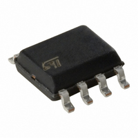
M93S46-WMN6TP STMicroelectronics, M93S46-WMN6TP Datasheet - Page 10

M93S46-WMN6TP
Manufacturer Part Number
M93S46-WMN6TP
Description
IC EEPROM 1KBIT 2MHZ 8SOIC
Manufacturer
STMicroelectronics
Datasheet
1.M93S46-WMN6TP.pdf
(34 pages)
Specifications of M93S46-WMN6TP
Format - Memory
EEPROMs - Serial
Memory Type
EEPROM
Memory Size
1K (64 x 16)
Speed
2MHz
Interface
Microwire, 3-Wire Serial
Voltage - Supply
2.5 V ~ 5.5 V
Operating Temperature
-40°C ~ 85°C
Package / Case
8-SOIC (3.9mm Width)
Organization
64 K x 16
Interface Type
Microwire
Maximum Clock Frequency
2 MHz
Supply Voltage (max)
5.5 V
Supply Voltage (min)
2.5 V
Maximum Operating Current
2 mA
Maximum Operating Temperature
+ 85 C
Mounting Style
SMD/SMT
Minimum Operating Temperature
- 40 C
Operating Supply Voltage
3.3 V, 5 V
Density
1Kb
Frequency (max)
2MHz
Write Protection
Yes
Data Retention
40Year
Operating Supply Voltage (typ)
3.3/5V
Package Type
SOIC N
Operating Temp Range
-40C to 85C
Supply Current
2mA
Operating Supply Voltage (min)
2.5V
Operating Supply Voltage (max)
5.5V
Operating Temperature Classification
Industrial
Mounting
Surface Mount
Pin Count
8
Lead Free Status / RoHS Status
Lead free / RoHS Compliant
Other names
497-8666-2
M93S46-WMN6TP
M93S46-WMN6TP
Available stocks
Company
Part Number
Manufacturer
Quantity
Price
Part Number:
M93S46-WMN6TP
Manufacturer:
ST
Quantity:
20 000
M93S66, M93S56, M93S46
Figure 5. PAWRITE and WRAL Sequence
Note: For the meanings of An, Xn and Dn, please see
Page Write
A Page Write to Memory (PAWRITE) instruction
contains the first address to be written, followed by
up to 4 data words.
After the receipt of each data word, bits A1-A0 of
the internal address register are incremented, the
high order bits remaining unchanged (A7-A2 for
M93S66, M93S56; A5-A2 for M93S46). Users
must take care, in the software, to ensure that the
last word address has the same upper order ad-
dress bits as the initial address transmitted to
avoid address roll-over.
10/34
PAGE
WRITE
WRITE
ALL
PRE
W
S
Q
PRE
W
S
Q
D
D
1 1
1 0
CODE
CODE
OP
OP
1
0
0 1
An
ADDR
ADDR
Xn X0
Table 2.
A0
Dn
Dn
and
Table
DATA IN
DATA IN
The Page Write to Memory (PAWRITE) instruction
will not be executed if any of the 4 words address-
es the protected area.
Write Enable (W) must be held High before and
during the instruction. Input address and data, on
Serial Data Input (D) are sampled on the rising
edge of Serial Clock (C).
After the last data bit has been sampled, the Chip
Select Input (S) must be taken Low before the next
rising edge of Serial Clock (C). If Chip Select Input
(S) is brought Low before or after this specific time
frame, the self-timed programming cycle will not
3..
D0
D0
BUSY
BUSY
STATUS
STATUS
CHECK
CHECK
READY
READY
AI00890C


