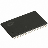
CY7C1021DV33-10ZSXI Cypress Semiconductor Corp, CY7C1021DV33-10ZSXI Datasheet - Page 6

CY7C1021DV33-10ZSXI
Manufacturer Part Number
CY7C1021DV33-10ZSXI
Description
IC SRAM 1MBIT 10NS 44TSOP
Manufacturer
Cypress Semiconductor Corp
Type
Asynchronousr
Datasheet
1.CY7C1021DV33-10VXI.pdf
(13 pages)
Specifications of CY7C1021DV33-10ZSXI
Memory Size
1M (64K x 16)
Package / Case
44-TSOP II
Format - Memory
RAM
Memory Type
SRAM - Asynchronous
Speed
10ns
Interface
Parallel
Voltage - Supply
3 V ~ 3.6 V
Operating Temperature
-40°C ~ 85°C
Access Time
10 ns
Supply Voltage (max)
3.6 V
Supply Voltage (min)
3 V
Maximum Operating Current
80 mA
Organization
64 K x 16
Maximum Operating Temperature
+ 85 C
Minimum Operating Temperature
- 40 C
Mounting Style
SMD/SMT
Number Of Ports
1
Operating Supply Voltage
3.3 V
Lead Free Status / RoHS Status
Lead free / RoHS Compliant
Lead Free Status / RoHS Status
Lead free / RoHS Compliant, Lead free / RoHS Compliant
Other names
428-1974
CY7C1021DV33-10ZSXI
CY7C1021DV33-10ZSXI
Available stocks
Company
Part Number
Manufacturer
Quantity
Price
Company:
Part Number:
CY7C1021DV33-10ZSXI
Manufacturer:
CY
Quantity:
420
Part Number:
CY7C1021DV33-10ZSXI
Manufacturer:
CYPRESS
Quantity:
20 000
Company:
Part Number:
CY7C1021DV33-10ZSXIT
Manufacturer:
ST
Quantity:
15 000
Company:
Part Number:
CY7C1021DV33-10ZSXIT
Manufacturer:
CYPRESS
Quantity:
1 364
Document #: 38-05460 Rev. *F
Data Retention Waveform
Data Retention Characteristics
Switching Waveforms
Read Cycle No. 1 (Address Transition Controlled)
Read Cycle No. 2 (OE Controlled)
Notes
V
I
t
t
13. Full device operation requires linear V
14. Device is continuously selected. OE, CE, BHE and/or BLE = V
15. WE is HIGH for Read cycle.
16. Address valid prior to or coincident with CE transition LOW.
Parameter
DATA OUT
CCDR
CDR
R
ADDRESS
CURRENT
DR
[13]
BHE, BLE
DATA OUT
ADDRESS
SUPPLY
[5]
V
V
OE
CE
CC
CE
CC
V
Data Retention Current
Chip Deselect to Data Retention Time
Operation Recovery Time
CC
for Data Retention
PREVIOUS DATA VALID
HIGH IMPEDANCE
Description
t
t
LZCE
PU
CC
ramp from V
[15, 16]
t
ACE
t
t
LZBE
t
DBE
LZOE
t
DOE
Over the Operating Range
t
50%
OHA
t
CDR
3.0V
DR
to V
IL
t
CC(min.)
AA
.
V
V
[14, 15]
CC
IN
> V
= V
> 50 s or stable at V
t
RC
CC
DR
DATA RETENTION MODE
= 2.0V, CE > V
– 0.3V or V
t
RC
RC
V
DR
>
Conditions
CC(min.)
2V
IN
DATA VALID
< 0.3V
CC
> 50 s.
– 0.3V,
Industrial
Automotive
t
HZOE
DATA VALID
3.0V
t
R
t
t
CY7C1021DV33
HZCE
HZBE
t
PD
Min.
t
RC
2
0
50%
IMPEDANCE
Max.
HIGH
15
3
Page 6 of 13
Unit
mA
mA
ns
ns
V
I
I
CC
SB
[+] Feedback


