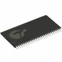
CY7C1061AV33-10ZXC Cypress Semiconductor Corp, CY7C1061AV33-10ZXC Datasheet - Page 4

CY7C1061AV33-10ZXC
Manufacturer Part Number
CY7C1061AV33-10ZXC
Description
IC SRAM 16MBIT 10NS 54TSOP
Manufacturer
Cypress Semiconductor Corp
Type
Asynchronousr
Datasheet
1.CY7C1061AV33-10ZXI.pdf
(14 pages)
Specifications of CY7C1061AV33-10ZXC
Memory Size
16M (1M x 16)
Package / Case
54-TSOP II
Interface
Parallel
Format - Memory
RAM
Memory Type
SRAM - Asynchronous
Speed
10ns
Voltage - Supply
3 V ~ 3.6 V
Operating Temperature
0°C ~ 70°C
Access Time
10 ns
Supply Voltage (max)
3.6 V
Supply Voltage (min)
3 V
Maximum Operating Current
275 mA
Organization
1 M x 16
Maximum Operating Temperature
+ 70 C
Minimum Operating Temperature
- 40 C
Mounting Style
SMD/SMT
Number Of Ports
1
Operating Supply Voltage
3.3 V
Density
16Mb
Access Time (max)
10ns
Sync/async
Asynchronous
Architecture
Not Required
Clock Freq (max)
Not RequiredMHz
Operating Supply Voltage (typ)
3.3V
Address Bus
20b
Package Type
TSOP-II
Operating Temp Range
0C to 70C
Supply Current
275mA
Operating Supply Voltage (min)
3V
Operating Supply Voltage (max)
3.6V
Operating Temperature Classification
Commercial
Mounting
Surface Mount
Pin Count
54
Word Size
16b
Number Of Words
1M
Memory Configuration
1M X 16
Supply Voltage Range
3V To 3.6V
Memory Case Style
TSOP
No. Of Pins
54
Operating Temperature Range
0°C To +70°C
Rohs Compliant
Yes
Lead Free Status / RoHS Status
Lead free / RoHS Compliant
Lead Free Status / RoHS Status
Lead free / RoHS Compliant, Lead free / RoHS Compliant
Other names
428-1983
CY7C1061AV33-10ZXC
CY7C1061AV33-10ZXC
Available stocks
Company
Part Number
Manufacturer
Quantity
Price
Company:
Part Number:
CY7C1061AV33-10ZXC
Manufacturer:
INFINEON
Quantity:
1 450
Maximum Ratings
Exceeding maximum ratings may shorten the useful life of the
device. These user guidelines are not tested.
Storage Temperature ............................... –65 C to +150 C
Ambient Temperature with
Power Applied .......................................... –55 C to +125 C
Supply Voltage on V
DC Voltage Applied to Outputs
in High Z State
DC Electrical Characteristics
(Over the Operating Range)
Capacitance
AC Test Loads and Waveforms
Notes
Document #: 38-05256 Rev. *K
V
V
V
V
I
I
I
I
I
C
C
3. V
4. Tested initially and after any design or process changes that may affect these parameters.
5. Valid SRAM operation does not occur until the power supplies have reached the minimum operating V
IX
OZ
CC
SB1
SB2
Parameter
Parameter
OH
OL
IH
IL
IN
OUT
minimum operating V
IL
OUTPUT
(min) = –2.0 V for pulse durations of less than 20 ns.
Output HIGH Voltage
Output LOW Voltage
Input HIGH Voltage
Input LOW Voltage
Input Leakage Current
Output Leakage Current
V
Automatic CE Power-down
Current —TTL Inputs
Automatic CE Power-down
Current —CMOS Inputs
Input Capacitance
I/O Capacitance
[3]
CC
................................. –0.5 V to V
[4]
Description
Operating Supply Current
Z
DD
CC
0
, normal SRAM operation can begin including reduction in V
= 50
to Relative GND
Rise time > 1 V/ns
Description
(a)
GND
3.3 V
[3]
30 pF* * Capacitive Load consists of all
50
T
A
= 25 C, f = 1 MHz, V
[3]
..–0.5 V to +4.6 V
components of the test environment.
[5]
V
10%
TH
Test Conditions
90%
CC
ALL INPUT PULSES
= 1.5 V
I
I
GND < V
GND < V
V
CE
V
CE
CE > V
V
or V
OH
OL
CC
IN
IN
+ 0.5 V
2
2
= 8.0 mA
= –4.0 mA
> V
> V
IN
= max, f = f
< V
< 0.3 V, Max V
(c)
< 0.3 V, f = 0
CC
IH
CC
IL,
I
O
or V
< V
– 0.3 V,
CC
– 0.3 V,
Max V
< V
Test Conditions
CC
= 3.3 V
IN
CC
max
< V
, Output Disabled
DC Input Voltage
Current into Outputs (LOW)......................................... 20 mA
Operating Range
CC
Commercial
Industrial
DD
CC
, CE > V
IL
= 1/t
to the data retention (V
, f = f
,
90%
Range
RC
10%
Fall time:
> 1 V/ns
max
IH
Commercial
Industrial
,
Commercial/
Industrial
TSOP II
DD
6
8
(3.0 V). As soon as 1 ms (T
[3]
OUTPUT
............................. –0.5 V to V
CCDR
INCLUDING
JIG AND
SCOPE
–40 C to +85 C
3.3 V
0 C to +70 C
Temperature
, 2.0 V) voltage.
Ambient
5 pF*
FBGA
–0.3
Min
2.4
2.0
–1
–1
–
–
–
–
–
10
8
(b)
R1 317
CY7C1061AV33
power
–10
V
) after reaching the
CC
Max
3.3 V 0.3 V
275
275
0.4
0.8
+1
+1
70
50
–
+ 0.3
351
Unit
R2
pF
pF
CC
V
Page 4 of 14
CC
+ 0.5 V
Unit
mA
mA
mA
mA
A
A
V
V
V
V
[+] Feedback


