N25S830HAT22I ON Semiconductor, N25S830HAT22I Datasheet
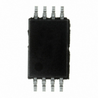
IC SRAM 256KBIT 20MHZ 8TSSOP

N25S830HAT22I

Manufacturer Part Number
N25S830HAT22I
Description
IC SRAM 256KBIT 20MHZ 8TSSOP
Manufacturer
ON Semiconductor
Type
Synchronousr
Datasheet

Specifications of N25S830HAT22I

Format - Memory
RAM
Memory Type
SRAM
Memory Size
256K (32K x 8)
Speed
20MHz
Interface
SPI Serial
Voltage - Supply
2.7 V ~ 3.6 V
Operating Temperature
-40°C ~ 85°C
Package / Case
8-TSSOP
Access Time
25 ns
Maximum Clock Frequency
20 MHz
Supply Voltage (max)
3.6 V
Supply Voltage (min)
2.7 V
Maximum Operating Current
3 mA
Organization
32 K x 8
Maximum Operating Temperature
+ 85 C
Minimum Operating Temperature
- 40 C
Mounting Style
SMD/SMT
Number Of Ports
1
Operating Supply Voltage
3 V
Lead Free Status / RoHS Status
Lead free / RoHS Compliant
Other names
766-1044

Available stocks

Company
Part Number
Manufacturer
Quantity
Price
Part Number:
N25S830HAT22I
Manufacturer:
ON/安森美
Quantity:
20 000
Company:
Part Number:
N25S830HAT22I
Quantity:
5 000
N25S830HA
256 Kb Low Power Serial
SRAMs
32 K x 8 Bit Organization
Introduction
integrated memory devices including this 256 Kb serially accessed
Static Random Access Memory, internally organized as 32 K words by
8 bits. The devices are designed and fabricated using
ON Semiconductor’s advanced CMOS technology to provide both
high−speed performance and low power. The devices operate with a
single chip select (CS) input and use a simple Serial Peripheral
Interface (SPI) serial bus. A single data in and data out line is used
along with a clock to access data within the devices. The N25S830HA
devices include a HOLD pin that allows communication to the device
to be paused. While paused, input transitions will be ignored. The
devices can operate over a wide temperature range of −40°C to +85°C
and can be available in several standard package offerings.
Features
© Semiconductor Components Industries, LLC, 2010
October, 2010 − Rev. 9
The ON Semiconductor serial SRAM family includes several
Single chip select (CS)
Serial input (SI) and serial output (SO)
Word read and write
Page mode (32 word page)
Burst mode (full array)
Compliant
Power Supply Range: 2.7 to 3.6 V
Very Low Standby Current: Typical Isb as low as 1 mA
Very Low Operating Current: As low as 3 mA
Simple Memory Control:
Flexible Operating Modes:
Organization: 32 K x 8 bit
Self Timed Write Cycles
Built−in Write Protection (CS High)
HOLD Pin for Pausing Communication
High Reliability: Unlimited write cycles
Green SOIC and TSSOP
These Devices are Pb−Free, Halogen Free/BFR Free and are RoHS
1
†For information on tape and reel specifications,
N25S830HAS22I
N25S830HAT22I
N25S830HAS22IT
N25S830HAT22IT
including part orientation and tape sizes, please
refer to our Tape and Reel Packaging Specification
Brochure, BRD8011/D.
VSS
N25S830HA
XXXXYZZ
Device
CS
SO
NC
CASE 948AL
PACKAGE CONFIGURATIONS
VSS
TSSOP−8
T SUFFIX
ORDERING INFORMATION
SO
NC
CS
1
MARKING DIAGRAM
http://onsemi.com
1
(Top Views)
(Pb−Free)
TSSOP−8
(Pb−Free)
(Pb−Free)
TSSOP−8
(Pb−Free)
TSSOP
Package
N25S830HA = Device Code
XXXX
Y
ZZ
G
SOIC−8
SOIC−8
SOIC
Publication Order Number:
CASE 751BD
S SUFFIX
= Wafer Lot
= Year
= Work Week
= Pb−Free
SOIC−8
__ / Tape & Reel
__ / Tape & Reel
__ Units / Tray
__ Units / Tray
N25S830HA/D
Shipping
HOLD
VCC
SCK
SI
HOLD
VCC
SCK
SI

Related parts for N25S830HAT22I

N25S830HAT22I Summary of contents

Page 1

... N25S830HAS22I SOIC−8 (Pb−Free) N25S830HAT22I TSSOP−8 (Pb−Free) N25S830HAS22IT SOIC−8 (Pb−Free) N25S830HAT22IT TSSOP−8 (Pb−Free) †For information on tape and reel specifications, including part orientation and tape sizes, please refer to our Tape and Reel Packaging Specification Brochure, BRD8011/D. 1 SOIC−8 S SUFFIX ...

Page 2

Table 1. DEVICE OPTIONS Supply (V) Part Number Density N25S830HAS2 256 Kb N25S830HAT2 Table 2. PIN NAMES Pin Name Pin Function CS Chip Select Input SCK Serial Clock Input SI Serial Data Input SO Serial Data Output HOLD Hold Input ...

Page 3

Table 3. ABSOLUTE MAXIMUM RATINGS Item Voltage on any pin relative Voltage on V Supply Relative Power Dissipation Storage Temperature Operating Temperature Soldering Temperature and Time Stresses exceeding Maximum Ratings may damage the ...

Page 4

Table 6. TIMING TEST CONDITIONS Item Input Pulse Level Input Rise and Fall Time Input and Output Timing Reference Levels Output Load Operating Temperature Table 7. TIMING Item Clock Frequency Clock Rise Time Clock Fall Time Clock High Time Clock ...

Page 5

CSS SCK MSB SCK MSB out SCK n+2 n n+2 n+1 n HOLD ...

Page 6

... When CS is high high−Z. CS must be driven low after power−up prior to any sequence being started. SCK Serial Clock I Synchronizes all activities between the memory and controller. All incoming addresses, data and instructions are latched on the rising edge of SCK. Data out is updated on SO after the falling edge of SCK. SI Serial Data In I Receives instructions, addresses and data on the rising edge of SCK ...

Page 7

SCK Instruction High− SCK Instruction High−Z SO ...

Page 8

... First, the 8−bit WRITE instruction is transmitted to the device followed by the 16−bit address with the MSB being a don’t care. After the WRITE instruction and addresses are sent, the data to be stored in memory is shifted in on the SI pin. If operating in page mode, after the initial word of data is shifted in, additional data words can be written as long as the address requested is sequential on the same page ...

Page 9

SCK Instruction Data In to ADDR ...

Page 10

WRITE Status Register Instruction (WRSR) This instruction provides the ability to write the status register and select among several operating modes. Several of the register bits must be set to a low ‘0’ if any of the other CS 0 ...

Page 11

E1 e TOP VIEW SIDE VIEW Notes: (1) All dimensions are in millimeters. Angles in degrees. (2) Complies with JEDEC MO-153. PACKAGE DIMENSIONS TSSOP8, 4.4x3 CASE 948AL−01 ISSUE O SYMBOL MIN A A1 0.05 A2 ...

Page 12

... Opportunity/Affirmative Action Employer. This literature is subject to all applicable copyright laws and is not for resale in any manner. PUBLICATION ORDERING INFORMATION LITERATURE FULFILLMENT: Literature Distribution Center for ON Semiconductor P.O. Box 5163, Denver, Colorado 80217 USA Phone: 303−675−2175 or 800−344−3860 Toll Free USA/Canada Fax: 303− ...

Related keywords