CY62148DV30LL-55SXI Cypress Semiconductor Corp, CY62148DV30LL-55SXI Datasheet
CY62148DV30LL-55SXI
Specifications of CY62148DV30LL-55SXI
CY62148DV30LL-55SXI


Related parts for CY62148DV30LL-55SXI

CY62148DV30LL-55SXI Summary of contents
Page 1
... Note 1. For best practice recommendations, refer to the Cypress application note “System Design Guidelines” on Cypress Semiconductor Corporation Document Number : 38-05341 Rev. *F 4-Mbit (512K x 8) MoBL Functional Description The CY62148DV30 is a high-performance CMOS static RAM organized as 512K words by 8 bits. This device features advanced circuit design to provide ultra-low active current. This is ideal for providing More Battery Life™ ...
Page 2
Contents Pin Configuration ............................................................. 3 Product Portfolio .............................................................. 3 Maximum Ratings ............................................................. 4 Operating Range ............................................................... 4 Electrical Characteristics ................................................. 4 Capacitance ...................................................................... 5 Thermal Resistance .......................................................... 5 AC Test Loads and Waveforms ....................................... 5 Data Retention Characteristics ....................................... 5 ...
Page 3
... Pin Configuration Product Portfolio Product Range Min CY62148DV30LL Industrial 2.2 Note 2. Typical values are included for reference only and are not guaranteed or tested. Typical values are measured at V Document Number : 38-05341 Rev. *F 32-pin SOIC Pinout Top View I I/O I I/O I I/O I/O ...
Page 4
... Full device AC operation assumes a 100 s ramp time from Document Number : 38-05341 Rev input voltage Output current into outputs (LOW) .............................. 20 mA Static discharge voltage........................................... > 2001V (per MIL-STD-883, method 3015) Latch-up current ..................................................... > 200 mA Operating Range Product + 0.3 V CC(max) CY62148DV30LL + 0.3 V CC(max) Test Conditions = –0 2. –1 2. ...
Page 5
Capacitance [6] Parameter Description C Input capacitance IN C Output capacitance OUT Thermal Resistance [6] Parameter Description Thermal resistance JA (Junction to ambient) Thermal resistance (Junction to JC case) AC Test Loads and Waveforms ...
Page 6
... HZOE HZCE HZWE 12. The internal write time of the memory is defined by the overlap of WE terminate a write by going INACTIVE. The data input set-up and hold timing should be referenced to the edge of the signal that terminates the write. 13. Device is continuously selected. OE ...
Page 7
Switching Waveforms (continued) Figure 2. Read Cycle No. 2 (OE Controlled) ADDRESS CE t ACE OE t LZOE HIGH IMPEDANCE DATA OUT t LZCE SUPPLY CURRENT Figure 3. Write Cycle No. 1 (WE Controlled) ADDRESS CE ...
Page 8
Switching Waveforms (continued) Figure 4. Write Cycle No. 2 (CE Controlled) ADDRESS DATA I/O Figure 5. Write Cycle No. 3 (WE Controlled, OE LOW) ADDRESS NOTE 22 DATA I/O t HZWE Truth ...
Page 9
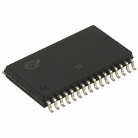
... Ordering Information Speed Ordering Code (ns) 55 CY62148DV30LL-55SXI Contact your local Cypress sales representative for availability of these parts Ordering Code Definition D V30 LL 621 Document Number : 38-05341 Rev. *F Package Package Type Diagram 51-85081 32-pin SOIC (Pb-free) I Temperature Grade Industrial Package Type pin SOIC (Pb-free) ...
Page 10
Package Diagrams MoBL is a registered trademark, and More Battery Life is a trademark, of Cypress Semiconductor. All product and company names mentioned in this document may be the trademarks of their respective holders. Document Number : 38-05341 Rev. *F ...
Page 11
... Acronyms Acronym Description CMOS complementary metal oxide semiconductor I/O input/output MoBL more battery life SOIC small-outline integrated circuit SRAM static random access memory Document Conventions Units of Measure Symbol Unit of Measure ns nano seconds V volts µA micro amperes mA milli amperes pF pico Farad °C ...
Page 12
Document History Page Document Title:CY62148DV30, 4-Mbit (512K x 8) MoBL Document Number: 38-05341 REV. ECN NO. Issue Date ** 127480 06/17/03 *A 131041 01/23/04 *B 222180 See ECN *C 498575 See ECN *D 729917 See ECN *E 2896036 03/19/10 *F ...
Page 13
... Cypress against all charges. Any Source Code (software and/or firmware) is owned by Cypress Semiconductor Corporation (Cypress) and is protected by and subject to worldwide patent protection (United States and foreign), United States copyright laws and international treaty provisions. Cypress hereby grants to licensee a personal, non-exclusive, non-transferable license to copy, use, modify, create derivative works of, and compile the Cypress Source Code and derivative works for the sole purpose of creating custom software and or firmware in support of licensee product to be used only in conjunction with a Cypress integrated circuit as specified in the applicable agreement ...