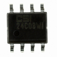
CAT93C86VI-G ON Semiconductor, CAT93C86VI-G Datasheet - Page 4

CAT93C86VI-G
Manufacturer Part Number
CAT93C86VI-G
Description
IC EEPROM 16KBIT 3MHZ 8SOIC
Manufacturer
ON Semiconductor
Datasheet
1.CAT93C86VI-GT3.pdf
(13 pages)
Specifications of CAT93C86VI-G
Format - Memory
EEPROMs - Serial
Memory Type
EEPROM
Memory Size
16K (2K x 8 or 1K x 16)
Speed
3MHz
Interface
Microwire, 3-Wire Serial
Voltage - Supply
1.8 V ~ 5.5 V
Operating Temperature
-40°C ~ 85°C
Package / Case
8-SOIC (3.9mm Width)
Organization
2 K x 8 or 1 K x 16
Interface Type
Microwire
Maximum Clock Frequency
0.5 MHz
Supply Voltage (max)
5.5 V
Supply Voltage (min)
2.5 V
Maximum Operating Current
3 mA
Maximum Operating Temperature
+ 85 C
Mounting Style
SMD/SMT
Minimum Operating Temperature
- 40 C
Operating Supply Voltage
3.3 V, 5 V
Lead Free Status / RoHS Status
Lead free / RoHS Compliant
Available stocks
Company
Part Number
Manufacturer
Quantity
Price
Part Number:
CAT93C86VI-G
Manufacturer:
CATALYST
Quantity:
20 000
Part Number:
CAT93C86VI-GT3
Manufacturer:
CATALYS
Quantity:
20 000
CAT93C86 (Rev. C)
INSTRUCTION SET
DEVICE OPERATION
The CAT93C86 is a 16,384-bit nonvolatile memory
intended
microprocessors. The CAT93C86 can be organized
as either registers of 16 bits or 8 bits. When organized
as X16, seven 13-bit instructions control the reading,
writing and erase operations of the device.
organized as X8, seven 14-bit instructions control the
reading, writing and erase operations of the device.
The CAT93C86 operates on a single power supply
and will generate on chip, the high voltage required
during any write operation.
Instructions, addresses, and write data are clocked
into the DI pin on the rising edge of the clock (SK).
The DO pin is normally in a high impedance state
except when reading data from the device, or when
checking the ready/busy status after a write operation.
The ready/busy status can be determined after the
start of a write operation by selecting the device (CS
high) and polling the DO pin; DO low indicates that the
write operation is not completed, while DO high
indicates that the device is ready for the next
instruction. If necessary, the DO pin may be placed
back into a high impedance state during chip select by
shifting a dummy “1” into the DI pin. The DO pin will
enter the high impedance state on the falling edge of
the clock (SK). Placing the DO pin into the high
impedance state is recommended in applications
where the DI pin and the DO pin are to be tied
together to form a common DI/O pin.
The format for all instructions sent to the device is a
logical “1” start bit, a 2-bit (or 4-bit) opcode, 10-bit
address (an additional bit when organized X8) and for
write operations a 16-bit data field (8-bit for X8
organizations).
Note: The Write, Erase, Write all and Erase all
instructions require PE=1. If PE is left floating, 93C86
Doc. No. MD-1091 Rev. R
Instruction
ERASE
WRITE
EWEN
EWDS
WRAL
READ
ERAL
for
Start
Bit
1
1
1
1
1
1
1
use
Opcode
10
11
01
00
00
00
00
with
industry
11XXXXXXXXX
00XXXXXXXXX
10XXXXXXXXX
01XXXXXXXXX
A10-A0
A10-A0
A10-A0
x8
standard
Address
When
11XXXXXXXX
00XXXXXXXX
10XXXXXXXX
01XXXXXXXX
4
A9-A0
A9-A0
A9-A0
x16
is in Program Enabled mode. For Write Enable and
Write Disable instruction PE = don’t care.
Read
Upon receiving a READ command and an address
(clocked into the DI pin), the DO pin of the CAT93C86
will come out of the high impedance state and, after
sending an initial dummy zero bit, will begin shifting
out the data addressed (MSB first). The output data
bits will toggle on the rising edge of the SK clock and
are stable after the specified time delay (t
After the initial data word has been shifted out and CS
remains asserted with the SK clock continuing to
toggle, the device will automatically increment to the
next address and shift out the next data word in a
sequential
continuously asserted and SK continues to toggle, the
device will keep incrementing to the next address
automatically until it reaches to the end of the address
space, then loops back to address 0.
sequential READ mode, only the initial data word is
preceeded by a dummy zero bit. All subsequent data
words will follow without a dummy zero bit.
Write
After receiving a WRITE command, address and the
data, the CS (Chip Select) pin must be deselected for
a minimum of t
the self clocking clear and data store cycle of the
memory location specified in the instruction. The
clocking of the SK pin is not necessary after the
device has entered the self clocking mode. The
ready/busy
determined by selecting the device and polling the DO
pin. Since this device features Auto-Clear before
write, it is NOT necessary to erase a memory location
before it is written into.
D7-D0
D7-D0
x8
READ
status
CSMIN
Data
D15-D0
D15-D0
. The falling edge of CS will start
mode.
x16
of
Characteristics subject to change without notice
the
Read Address AN– A0
Clear Address AN– A0
Write Address AN– A0
Write Enable
Write Disable
Clear All Addresses
Write All Addresses
As
CAT93C86
© 2008 SCILLC. All rights reserved
long
Comments
PD0
as
or t
can
CS
In the
PD1
).
be
is


