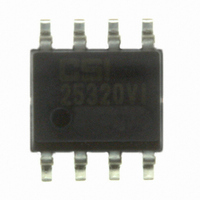
CAT25320VI-G ON Semiconductor, CAT25320VI-G Datasheet - Page 5

CAT25320VI-G
Manufacturer Part Number
CAT25320VI-G
Description
IC EEPROM 32KBIT 10MHZ 8SOIC
Manufacturer
ON Semiconductor
Datasheet
1.CAT25320VI-GT3.pdf
(16 pages)
Specifications of CAT25320VI-G
Format - Memory
EEPROMs - Serial
Memory Type
EEPROM
Memory Size
32K (4K x 8)
Speed
10MHz
Interface
SPI, 3-Wire Serial
Voltage - Supply
1.8 V ~ 5.5 V
Operating Temperature
-40°C ~ 85°C
Package / Case
8-SOIC (3.9mm Width)
Organization
4 K x 8
Interface Type
SPI
Maximum Clock Frequency
5 MHz
Access Time
75 ns
Supply Voltage (max)
5.5 V
Supply Voltage (min)
1.8 V
Maximum Operating Current
3 mA
Maximum Operating Temperature
+ 85 C
Mounting Style
SMD/SMT
Minimum Operating Temperature
- 40 C
Operating Supply Voltage
1.8 V, 5.5 V
Lead Free Status / RoHS Status
Lead free / RoHS Compliant
Available stocks
Company
Part Number
Manufacturer
Quantity
Price
Company:
Part Number:
CAT25320VI-GT3
Manufacturer:
ON Semiconductor
Quantity:
3 500
Part Number:
CAT25320VI-GT3
Manufacturer:
ON/安森美
Quantity:
20 000
Status Register
number of status and control bits.
with a write operation. This bit is automatically set to 1 during
an internal write cycle, and reset to 0 when the device is ready
to accept commands. For the host, this bit is read only.
WREN/WRDI commands. When set to 1, the device is in a
Write Enable state and when set to 0, the device is in a Write
Disable state.
blocks are currently write protected. They are set by the user
with the WRSR command and are non−volatile. The user is
Table 8. STATUS REGISTER
Table 9. BLOCK PROTECTION BITS
Table 10. WRITE PROTECT CONDITIONS
The Status Register, as shown in Table 8, contains a
The RDY (Ready) bit indicates whether the device is busy
The WEL (Write Enable Latch) bit is set/reset by the
The BP0 and BP1 (Block Protect) bits determine which
WPEN
7
WPEN
BP1
X
X
0
0
1
1
0
0
1
1
Status Register Bits
6
0
High
High
Low
Low
WP
BP0
X
X
0
1
0
1
5
0
WEL
0
1
0
1
0
1
Array Address Protected
http://onsemi.com
4
0
0C00−0FFF
0800−0FFF
0000−0FFF
None
5
Protected Blocks
allowed to protect a quarter, one half or the entire memory,
by setting these bits according to Table 9. The protected
blocks then become read−only.
the WP pin. Hardware write protection is enabled when the
WP pin is low and the WPEN bit is 1. This condition
prevents writing to the status register and to the block
protected sections of memory. While hardware write
protection is active, only the non−block protected memory
can be written. Hardware write protection is disabled when
the WP pin is high or the WPEN bit is 0. The WPEN bit, WP
pin and WEL bit combine to either permit or inhibit Write
operations, as detailed in Table 10.
Protected
Protected
Protected
Protected
Protected
Protected
The WPEN (Write Protect Enable) bit acts as an enable for
BP1
3
Unprotected Blocks
BP0
2
Protected
Protected
Protected
Writable
Writable
Writable
Quarter Array Protection
Half Array Protection
Full Array Protection
No Protection
Protection
WEL
1
Status Register
Protected
Protected
Protected
Protected
Writable
Writable
RDY
0


