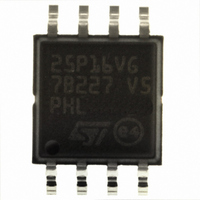
M25P16-VMW6TG NUMONYX, M25P16-VMW6TG Datasheet - Page 33

M25P16-VMW6TG
Manufacturer Part Number
M25P16-VMW6TG
Description
IC FLASH 16MBIT 75MHZ 8SOIC
Manufacturer
NUMONYX
Series
Forté™r
Datasheet
1.M25P16-VMN6P.pdf
(59 pages)
Specifications of M25P16-VMW6TG
Format - Memory
FLASH
Memory Type
FLASH
Memory Size
16M (2M x 8)
Speed
75MHz
Interface
SPI, 3-Wire Serial
Voltage - Supply
2.7 V ~ 3.6 V
Operating Temperature
-40°C ~ 85°C
Package / Case
8-SOIC (5.3mm Width), 8-SOP, 8-SOEIAJ
Package
8SOIC W
Cell Type
NOR
Density
16 Mb
Architecture
Sectored
Block Organization
Symmetrical
Typical Operating Supply Voltage
3.3 V
Sector Size
64KByte x 32
Timing Type
Synchronous
Interface Type
Serial-SPI
Lead Free Status / RoHS Status
Lead free / RoHS Compliant
Other names
M25P16-VMW6TG
M25P16-VMW6TGTR
M25P16-VMW6TGTR
Available stocks
Company
Part Number
Manufacturer
Quantity
Price
Company:
Part Number:
M25P16-VMW6TG
Manufacturer:
ST
Quantity:
53 700
Company:
Part Number:
M25P16-VMW6TG
Manufacturer:
Numonyx
Quantity:
45 000
Part Number:
M25P16-VMW6TG
Manufacturer:
ST
Quantity:
20 000
Figure 19. Release from Deep Power-down and Read Electronic Signature (RES) instruction
1. The value of the 8-bit electronic signature, for the M25P16, is 14h.
Figure 20. Release from Deep Power-down (RES) instruction sequence
Driving Chip Select (S) High after the 8-bit instruction byte has been received by the device, but before
the whole of the 8-bit electronic signature has been transmitted for the first time (as shown in
still ensures that the device is put into Standby Power mode. If the device was not previously in the Deep
Power-down mode, the transition to the Standby Power mode is immediate. If the device was previously
in the Deep Power-down mode, though, the transition to the Standby Power mode is delayed by t
and Chip Select (S) must remain High for at least t
device waits to be selected, so that it can receive, decode and execute instructions.
S
C
D
Q
S
C
D
Q
0
sequence and data-out sequence
1
High Impedance
2
Instruction
3
High Impedance
0
4
1
5
2
6
Instruction
3
7
MSB
23
4
8
22 21
5
9 10
3 Dummy bytes
6
7
3
28 29 30 31 32 33 34 35
2
RES1
1
Deep Power-down mode
0
(max). Once in the Standby Power mode, the
MSB
7
t
RES1
Electronic Signature Out
Deep Power-down mode
6
5
4
3
36 37 38
2
Standby mode
1
0
t
RES2
Standby mode
Figure
AI04078B
RES1
AI04047C
33/59
20),
,


