CAT28F020L12 ON Semiconductor, CAT28F020L12 Datasheet - Page 9
CAT28F020L12
Manufacturer Part Number
CAT28F020L12
Description
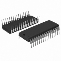
IC FLASH 2MBIT 120NS 32DIP
Manufacturer
ON Semiconductor
Datasheet
1.CAT28F020G-90T.pdf
(16 pages)
Specifications of CAT28F020L12
Format - Memory
FLASH
Memory Type
FLASH
Memory Size
2M (256K x 8)
Speed
120ns
Interface
Parallel
Voltage - Supply
4.5 V ~ 5.5 V
Operating Temperature
0°C ~ 70°C
Package / Case
32-DIP (0.600", 15.24mm)
Data Bus Width
8 bit
Architecture
Non Sectored
Interface Type
Parallel
Supply Voltage (max)
5.5 V
Supply Voltage (min)
4.5 V
Maximum Operating Current
30 mA
Mounting Style
Through Hole
Lead Free Status / RoHS Status
Lead free / RoHS Compliant
Other names
CAT28F020L-12
CAT28F020L-12
CAT28F020L-12
Available stocks
Company
Part Number
Manufacturer
Quantity
Price
Company:

Part Number:
CAT28F020L12
Manufacturer:
ON Semiconductor
Quantity:
135


WRITE OPERATIONS
The following operations are initiated by observing the
sequence specified in the Write Command Table.
Read Mode
The device can be put into a standard READ mode by
initiating a write cycle with 00H on the data bus. The
subsequent read cycles will be performed similar to a
standard EPROM or E
Signature Mode
An alternative method for reading device signature (see
Read Operations Signature Mode), is initiated by writing
the code 90H into the command register while keeping
V
OE low (and WE high) will output the device signature.
Figure 4. A.C. Timing for Erase Operation
© 2009 SCILLC. All rights reserved.
Characteristics subject to change without notice
ADDRESSES
PP
DATA (I/O)
high. A read cycle from address 0000H with CE and
WE (W)
OE (G)
CE (E)
V CC POWER-UP
CATALYST Code = 00110001 (31H)
V CC
V PP
& STANDBY
5.0V
0V
V PPH
V PPL
t GHWL
HIGH-Z
2
SETUP ERASE
PROM Read.
COMMAND
t VPEL
t DS
t WC
t CH
t WP
t CS
t WPH
DATA IN
= 20H
COMMAND
t DH
ERASE
t DS
t WC
DATA IN
= 20H
t WP
ERASING
t CH
9
t DH
t AS
t CS
t WHWH2
A Read cycle from address 0001H retrieves the binary
code for the device on outputs I/O
Erase Mode
During the first Write cycle, the command 20H is written
into the command register. In order to commence the
erase operation, the identical command of 20H has to be
written again into the register. This two-step process
ensures against accidental erasure of the memory con-
tents. The final erase cycle will be stopped at the rising
edge of WE, at which time the Erase Verify command
(A0H) is sent to the command register. During this cycle,
the address to be verified is sent to the address bus and
latched when WE goes low. An integrated stop timer
allows for automatic timing control over this operation,
eliminating the need for a maximum erase timing speci-
fication. Refer to AC Characteristics (Program/Erase)
for specific timing parameters.
ERASE VERIFY
COMMAND
t WP
t DS
t WC
28F020 Code = 1011 1101 (BDH)
t AH
DATA IN
= A0H
t DH
t CH
t WHGL
t OLZ
t OE
t LZ
t CE
VERIFICATION
ERASE
t RC
DATA OUT
0
VALID
to I/O
V CC POWER-DOWN/
Doc. No. MD-1029, Rev. F
CAT28F020
7
STANDBY
t EHQZ
t DF
.
t OH
28F020 F11
Related parts for CAT28F020L12
Image
Part Number
Description
Manufacturer
Datasheet
Request
R

Part Number:
Description:
ON Semiconductor [VOLTAGE REGULATOR]
Manufacturer:
ON Semiconductor
Datasheet:
Part Number:
Description:
357-036-542-201 CARDEDGE 36POS DL .156 BLK LOPRO
Manufacturer:
ON Semiconductor
Datasheet:
Part Number:
Description:
357-036-542-201 CARDEDGE 36POS DL .156 BLK LOPRO
Manufacturer:
ON Semiconductor
Datasheet:
Part Number:
Description:
357-036-542-201 CARDEDGE 36POS DL .156 BLK LOPRO
Manufacturer:
ON Semiconductor
Datasheet:
Part Number:
Description:
357-036-542-201 CARDEDGE 36POS DL .156 BLK LOPRO
Manufacturer:
ON Semiconductor
Datasheet:
Part Number:
Description:
357-036-542-201 CARDEDGE 36POS DL .156 BLK LOPRO
Manufacturer:
ON Semiconductor
Datasheet:
Part Number:
Description:
357-036-542-201 CARDEDGE 36POS DL .156 BLK LOPRO
Manufacturer:
ON Semiconductor
Datasheet:
Part Number:
Description:
357-036-542-201 CARDEDGE 36POS DL .156 BLK LOPRO
Manufacturer:
ON Semiconductor
Datasheet:
Part Number:
Description:
357-036-542-201 CARDEDGE 36POS DL .156 BLK LOPRO
Manufacturer:
ON Semiconductor
Datasheet:
Part Number:
Description:
357-036-542-201 CARDEDGE 36POS DL .156 BLK LOPRO
Manufacturer:
ON Semiconductor
Datasheet:
Part Number:
Description:
357-036-542-201 CARDEDGE 36POS DL .156 BLK LOPRO
Manufacturer:
ON Semiconductor
Datasheet:
Part Number:
Description:
Manufacturer:
ON Semiconductor
Datasheet:
Part Number:
Description:
Manufacturer:
ON Semiconductor
Datasheet:
Part Number:
Description:
Manufacturer:
ON Semiconductor
Datasheet: