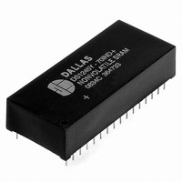
DS1248Y-70IND+ Maxim Integrated Products, DS1248Y-70IND+ Datasheet - Page 17

DS1248Y-70IND+
Manufacturer Part Number
DS1248Y-70IND+
Description
IC NVSRAM 1MBIT 70NS 32DIP
Manufacturer
Maxim Integrated Products
Datasheet
1.DS1248W-120.pdf
(18 pages)
Specifications of DS1248Y-70IND+
Format - Memory
RAM
Memory Type
NVSRAM (Non-Volatile SRAM)
Memory Size
1M (128K x 8)
Speed
70ns
Interface
Parallel
Voltage - Supply
4.5 V ~ 5.5 V
Operating Temperature
-40°C ~ 85°C
Package / Case
32-DIP Module (600 mil), 32-EDIP
Lead Free Status / RoHS Status
Lead free / RoHS Compliant
AC TEST CONDITIONS
Output Load: 50pF + 1TTL Gate
Input Pulse Levels: 0 to 3V
Timing Measurement Reference Levels
Input Pulse Rise and Fall Times: 5ns
NOTES:
1) WE is high for a read cycle.
2) OE = V
3) t
4) t
5) These parameters are sampled with a 50pF load and are not 100% tested.
6) If the CE low transition occurs simultaneously with or later than the WE low transition in Write Cycle
7) If the CE high transition occurs prior to or simultaneously with the WE high transition, the output
8) If WE is low or the WE low transition occurs prior to or simultaneously with the CE low transition,
9) The expected t
10) t
11) Voltages are referenced to ground.
12) RST (Pin 1) has an internal pullup resistor.
13) RTC modules can be successfully processed through conventional wave-soldering techniques as long
Input: 1.5V
Output: 1.5V
low to the earlier of CE or WE going high.
1, the output buffers remain in a high-impedance state during this period.
buffers remain in a high-impedance state during this period.
the output buffers remain in a high impedance state during this period.
running.
as temperature exposure to the lithium energy source contained within does not exceed +85°C. Post-
solder cleaning with water-washing techniques is acceptable, provided that ultrasonic vibration is not
used. See the PowerCap package drawing for details regarding the PowerCap package.
WP
DH
WR
, t
is specified as the logical AND of CE and WE. t
is a function of the latter occurring edge of WE or CE.
DS
IH
are measured from the earlier of CE or WE going high.
or V
IL
DR
. If CE = V
is defined as cumulative time in the absence of V
IH
during write cycle, the output buffers remain in a high impedance state.
17 of 18
WP
is measured from the latter of CE or WE going
CC
with the clock oscillator


