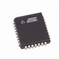
AT45DB161-JI Atmel, AT45DB161-JI Datasheet - Page 5

AT45DB161-JI
Manufacturer Part Number
AT45DB161-JI
Description
IC FLASH 16MBIT 13MHZ 32PLCC
Manufacturer
Atmel
Datasheet
1.AT45DB161-JC.pdf
(21 pages)
Specifications of AT45DB161-JI
Format - Memory
FLASH
Memory Type
DataFLASH
Memory Size
16M (4096 pages x 528 bytes)
Speed
13MHz
Interface
SPI, 3-Wire Serial
Voltage - Supply
2.7 V ~ 3.6 V
Operating Temperature
-40°C ~ 85°C
Package / Case
32-PLCC
Lead Free Status / RoHS Status
Contains lead / RoHS non-compliant
Other names
AT45DB161JI
Block Erase Addressing
MAIN MEMORY PAGE PROGRAM: This operation is a
combination of the Buffer Write and Buffer to Main Memory
Page Program with Built-in Erase operations. Data is first
shifted into buffer 1 or buffer 2 from the SI pin and then pro-
grammed into a specified page in the main memory. An
8-bit opcode, 82H for buffer 1 or 85H for buffer 2, is fol-
lowed by the two reserved bits and 22 address bits. The 12
most significant address bits (PA11-PA0) select the page in
the main memory where data is to be written, and the next
10 address bits (BFA9-BFA0) select the first byte in the
buffer to be written. After all address bits are shifted in, the
part will take data from the SI pin and store it in one of the
data buffers. If the end of the buffer is reached, the device
will wrap around back to the beginning of the buffer. When
there is a low-to-high transition on the CS pin, the part will
first erase the selected page in main memory to all 1s and
then program the data stored in the buffer into the specified
page in the main memory. Both the erase and the program-
ming of the page are internally self-timed and should take
place in a maximum of time t
register will indicate that the part is busy.
AUTO PAGE REWRITE: This mode is only needed if multi-
ple bytes within a page or multiple pages of data are
modified in a random fashion. This mode is a combination
of two operations: Main Memory Page to Buffer Transfer
and Buffer to Main Memory Page Program with Built-in
Erase. A page of data is first transferred from the main
memory to buffer 1 or buffer 2, and then the same data
(from buffer 1 or buffer 2) is programmed back into its origi-
nal page of main memory. An 8-bit opcode, 58H for buffer 1
or 59H for buffer 2, is followed by the two reserved bits, 12
address bits (PA11-PA0) that specify the page in main
memory to be rewritten, and 10 additional don’t care bits.
When a low-to-high transition occurs on the CS pin, the
part will first transfer data from the page in main memory to
PA11
0
0
0
0
1
1
1
1
•
•
•
PA10
0
0
0
0
1
1
1
1
•
•
•
PA9
0
0
0
0
1
1
1
1
•
•
•
EP
. During this time, the status
PA8
0
0
0
0
1
1
1
1
•
•
•
PA7
0
0
0
0
1
1
1
1
•
•
•
PA6
0
0
0
0
1
1
1
1
•
•
•
PA5
0
0
0
0
1
1
1
1
•
•
•
a buffer and then program the data from the buffer back
into same page of main memory. The operation is internally
self-timed and should take place in a maximum time of t
During this time, the status register will indicate that the
part is busy.
If a sector is programmed or reprogrammed sequentially
page by page, then the programming algorithm shown in
Figure 1 on page 17 is recommended. Otherwise, if multi-
ple bytes in a page or several pages are programmed
randomly in a sector, then the programming algorithm
shown in Figure 2 on page 18 is recommended.
STATUS REGISTER: The status register can be used to
determine the device’s ready/busy status, the result of a
Main Memory Page to Buffer Compare operation, or the
device density. To read the status register, an opcode of
57H must be loaded into the device. After the last bit of the
opcode is shifted in, the eight bits of the status register,
starting with the MSB (bit 7), will be shifted out on the SO
pin during the next eight clock cycles. The five most signifi-
cant bits of the status register will contain device
information, while the remaining three least significant bits
are reserved for future use and will have undefined values.
After bit 0 of the status register has been shifted out, the
sequence will repeat itself (as long as CS remains low and
SCK is being toggled) starting again with bit 7. The data in
the status register is constantly updated, so each repeating
sequence will output new data.
Ready/Busy status is indicated using bit 7 of the status reg-
ister. If bit 7 is a 1, then the device is not busy and is ready
to accept the next command. If bit 7 is a 0, then the device
is in a busy state. The user can continuously poll bit 7 of the
status register by stopping SCK once bit 7 has been output.
The status of bit 7 will continue to be output on the SO pin,
and once the device is no longer busy, the state of SO will
change from 0 to 1. There are eight operations which can
PA4
0
0
1
1
0
0
1
1
•
•
•
PA3
0
1
0
1
0
1
0
1
•
•
•
PA2
X
X
X
X
X
X
X
X
•
•
•
PA1
X
X
X
X
X
X
X
X
•
•
•
PA0
X
X
X
X
X
X
X
X
•
•
•
Block
508
509
510
511
0
1
2
3
•
•
•
EP
5
.


