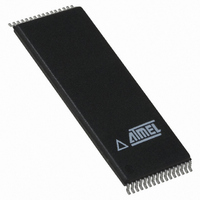
AT49F002T-12TC Atmel, AT49F002T-12TC Datasheet - Page 2

AT49F002T-12TC
Manufacturer Part Number
AT49F002T-12TC
Description
IC FLASH 2MBIT 120NS 32TSOP
Manufacturer
Atmel
Datasheet
1.AT49F002T-70VI.pdf
(17 pages)
Specifications of AT49F002T-12TC
Format - Memory
FLASH
Memory Type
FLASH
Memory Size
2M (256K x 8)
Speed
120ns
Interface
Parallel
Voltage - Supply
4.5 V ~ 5.5 V
Operating Temperature
0°C ~ 70°C
Package / Case
32-TSOP
Lead Free Status / RoHS Status
Contains lead / RoHS non-compliant
Other names
AT49F002T12TC
When the device is deselected, the CMOS standby current
is less than 100 µA. For the AT49F002N(T) pin 1 for the
DIP and PLCC packages and pin 9 for the TSOP package
are don’t connect pins.
To allow for simple in-system reprogrammability, the
AT49F002(N)(T) does not require high input voltages for
programming. Five-volt-only commands determine the read
and programming operation of the device. Reading data
out of the device is similar to reading from an EPROM; it
has standard CE, OE, and WE inputs to avoid bus conten-
tion. Reprogramming the AT49F002(N)(T) is performed by
erasing a block of data and then programming on a byte by
byte basis. The byte programming time is a fast 50 µs. The
end of a program cycle can be optionally detected by the
DATA polling feature. Once the end of a byte program
cycle has been detected, a new access for a read or pro-
gram can begin. The typical number of program and erase
cycles is in excess of 10,000 cycles.
Block Diagram
2
AT49F002(N)(T)
ADDRESS
INPUTS
RESET
GND
VCC
WE
OE
CE
Y DECODER
X DECODER
CONTROL
LOGIC
DATA INPUTS/OUTPUTS
DATA LATCHES
INPUT/OUTPUT
MAIN MEMORY
MAIN MEMORY
(128K BYTES)
BOOT BLOCK
PARAMETER
PARAMETER
AT49F002(N)
(96K BYTES)
(16K BYTES)
(8K BYTES)
(8K BYTES)
PROGRAM
Y-GATING
I/O7 - I/O0
BUFFERS
BLOCK 2
BLOCK 1
BLOCK 2
BLOCK 1
The device is erased by executing the erase command
sequence; the device internally controls the erase opera-
tions. There are two 8K byte parameter block sections and
two main memory blocks.
The device has the capability to protect the data in the boot
block; this feature is enabled by a command sequence.
The 16K-byte boot block section includes a reprogramming
lock out feature to provide data integrity. The boot sector is
designed to contain user secure code, and when the fea-
ture is enabled, the boot sector is protected from being
reprogrammed.
In the AT49F002(N)(T), once the boot block programming
lockout feature is enabled, the contents of the boot block
a r e p e r m a n e n t a n d c a n n o t b e c h a n g e d . I n t h e
AT49F002(T), once the boot block programming lockout
feature is enabled, the contents of the boot block cannot be
changed with input voltage levels of 5.5 volts or less.
8
3FFFF
20000
1FFFF
08000
07FFF
06000
05FFF
04000
03FFF
00000
DATA INPUTS/OUTPUTS
DATA LATCHES
INPUT/OUTPUT
MAIN MEMORY
MAIN MEMORY
AT49F002(N)T
(128K BYTES)
BOOT BLOCK
PARAMETER
PARAMETER
(16K BYTES)
(96K BYTES)
(8K BYTES)
(8K BYTES)
PROGRAM
Y-GATING
I/O7 - I/O0
BUFFERS
BLOCK 1
BLOCK 2
BLOCK 1
BLOCK 2
8
3FFFF
3C000
3BFFF
3A000
39FFF
38000
37FFF
20000
1FFFF
00000


