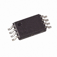
AT93C86-10TI-2.7 Atmel, AT93C86-10TI-2.7 Datasheet - Page 5

AT93C86-10TI-2.7
Manufacturer Part Number
AT93C86-10TI-2.7
Description
IC EEPROM 16KBIT 2MHZ 8TSSOP
Manufacturer
Atmel
Datasheet
1.AT93C86-10PC-2.7.pdf
(15 pages)
Specifications of AT93C86-10TI-2.7
Format - Memory
EEPROMs - Serial
Memory Type
EEPROM
Memory Size
16K (2K x 8 or 1K x 16)
Speed
1MHz, 2MHz
Interface
3-Wire Serial
Voltage - Supply
2.7 V ~ 5.5 V
Operating Temperature
-40°C ~ 85°C
Package / Case
8-TSSOP
Lead Free Status / RoHS Status
Contains lead / RoHS non-compliant
Available stocks
Company
Part Number
Manufacturer
Quantity
Price
Company:
Part Number:
AT93C86-10TI-2.7
Manufacturer:
AMC
Quantity:
5 000
Part Number:
AT93C86-10TI-2.7
Manufacturer:
ATMEL/爱特梅尔
Quantity:
20 000
Instruction Set for the AT93C86
Functional
Description
1237E–SEEPR–01/03
Instruction
READ
EWEN
ERASE
WRITE
ERAL
WRAL
EWDS
SB
1
1
1
1
1
1
1
Op Code
10
11
01
00
00
00
00
01XXXXXXXX
00XXXXXXXX
11XXXXXXXX
10XXXXXXXX
The AT93C86 is accessed via a simple and versatile 3-wire serial communication inter-
face. Device operation is controlled by seven instructions issued by the host processor.
A valid instruction starts with a rising edge of CS and consists of a Start Bit (logic
“1”) followed by the appropriate Op Code and the desired memory Address location.
READ (READ): The Read (READ) instruction contains the Address code for the mem-
ory location to be read. After the instruction and address are decoded, data from the
selected memory location is available at the serial output pin DO. Output data changes
are synchronized with the rising edges of serial clock SK. It should be noted that a
dummy bit (logic “0”) precedes the 8- or 16-bit data output string.
ERASE/WRITE (EWEN): To assure data integrity, the part automatically goes into the
Erase/Write Disable (EWDS) state when power is first applied. An Erase/Write Enable
(EWEN) instruction must be executed first before any programming instructions can be
carried out. Please note that once in the Erase/Write Enable state, programming
remains enabled until an Erase/Write Disable (EWDS) instruction is executed or V
power is removed from the part.
ERASE (ERASE): The Erase (ERASE) instruction programs all bits in the specified
memory location to the logical “1” state. The self-timed erase cycle starts once the
ERASE instruction and address are decoded. The DO pin outputs the READY/BUSY
status of the part if CS is brought high after being kept low for a minimum of 250 ns (t
A logic “1” at pin DO indicates that the selected memory location has been erased, and
the part is ready for another instruction.
WRITE (WRITE): The Write (WRITE) instruction contains the 8 or 16 bits of data to be
written into the specified memory location. The self-timed programming cycle, t
after the last bit of data is received at serial data input pin DI. The DO pin outputs the
READY/BUSY status of the part if CS is brought high after being kept low for a minimum
of 250 ns (t
“1” indicates that the memory location at the specified address has been written with the
data pattern contained in the instruction and the part is ready for further instructions. A
READY/BUSY status cannot be obtained if the CS is brought high after the end of
the self-timed programming cycle, t
A
A
A
10
10
10
x 8
- A
- A
- A
0
0
0
Address
CS
). A logic “0” at DO indicates that programming is still in progress. A logic
10XXXXXXXX
01XXXXXXXX
11XXXXXXXX
00XXXXXXXX
A
A
A
x 16
9
9
9 -
- A
- A
A
0
0
0
D
D
7
7
x 8
- D
- D
0
0
Data
WP
D
D
.
x 16
15
15
- D
- D
0
0
Comments
Reads data stored in memory,
at specified address.
programming modes.
Erases memory location A
Writes memory location A
Erases all memory locations.
Valid only at V
Writes all memory locations.
Valid when V
Disable Register cleared.
Write enable must precede all
Disables all programming instructions.
CC
CC
= 4.5V to 5.5V and
= 4.5V to 5.5V.
AT93C86
n
n
- A
- A
0
0
WP
.
.
, starts
CS
CC
).
5


