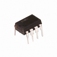
AT93C46A-10PU-2.7 Atmel, AT93C46A-10PU-2.7 Datasheet

AT93C46A-10PU-2.7
Specifications of AT93C46A-10PU-2.7
Available stocks
Related parts for AT93C46A-10PU-2.7
AT93C46A-10PU-2.7 Summary of contents
Page 1
... The AT93C46A is available in space-saving 8- lead PDIP, 8-lead JEDEC SOIC, and 8-lead TSSOP packages. The AT93C46A is enabled through the Chip Select pin (CS) and accessed via a three- wire serial interface consisting of Data Input (DI), Data Output (DO), and Shift Clock (SK). Upon receiving a Read instruction at DI, the address is decoded and the data is clocked out serially on the data output DO pin ...
Page 2
... Absolute Maximum Ratings* Operating Temperature......................................−55°C to +125°C Storage Temperature .........................................−65°C to +150°C Voltage on Any Pin with Respect to Ground ........................................ −1.0V to +7.0V Maximum Operating Voltage .......................................... 6.25V DC Output Current........................................................ 5.0 mA AT93C46A 2 *NOTICE: Figure 1. Block Diagram MEMORY ARRAY REGISTER DECODE GENERATOR Stresses beyond those listed under “Absolute Maximum Ratings” ...
Page 3
... V ≤ 5.5V CC 1.8V ≤ V ≤ 2.7V ≤ V ≤ 5. −0 0. 1.8V ≤ V ≤ 2. −100 µ AT93C46A = +5.0V (unless otherwise noted) CC Max Units Conditions +1.8V to +5.5V, (unless otherwise noted) CC Min Typ Max 1.8 5.5 2.7 5.5 4.5 5.5 0.5 2.0 0.5 2 ...
Page 4
... CS to Status Valid High t DF Impedance t Write Cycle Time WP (1) Endurance 5.0V, 25°C Note: 1. This parameter is characterized and is not 100% tested. AT93C46A 4 = −40° 85° Test Condition 4.5V ≤ V ≤ 5.5V CC 2.7V ≤ V ≤ 5.5V CC 1.8V ≤ V ≤ 5.5V CC 4.5V ≤ V ≤ ...
Page 5
... The AT93C46A is accessed via a simple and versatile three-wire serial communication interface. Device operation is controlled by seven instructions issued by the host pro- cessor. A valid instruction starts with a rising edge of CS and consists of a start bit (logic “1”) followed by the appropriate op code and the desired memory address location. ...
Page 6
... Erase/Write Disable (EWDS) instruction disables all programming modes and should be executed after all programming operations. The operation of the Read instruction is independent of both the EWEN and EWDS instructions and can be executed at any time. µ s (1) Table 6. Organization Key for Timing Diagrams I 5.0V ± 10%. CC AT93C46A 0539J–SEEPR–11/ ...
Page 7
... Figure 3. READ Timing High Impedance 1 Figure 4. EWEN Timing Note: 1. Requires a minimum of nine clock cycles. 1 Figure 5. EWDS Timing Note: 1. Requires a minimum of nine clock cycles. 0539J–SEEPR–11/04 ... ... AT93C46A ...
Page 8
... Figure 6. WRITE Timing HIGH IMPEDANCE DO (1 ),( 2 ) Figure 7. WRAL Timing HIGH IMPEDANCE DO Notes: 1. Valid only 4.5V to 5.5V Requires a minimum of nine clock cycles. Figure 8. ERASE Timing HIGH IMPEDANCE DO AT93C46A 8 ... ... ... ... N N-1 N BUSY READY ... D0 N BUSY READY STANDBY CHECK STATUS HIGH IMPEDANCE BUSY READY ...
Page 9
... Figure 9. ERAL Timing HIGH IMPEDANCE DO Note: 1. Valid only 4.5V to 5.5V. CC 0539J–SEEPR–11/ AT93C46A t CS STANDBY CHECK STATUS BUSY HIGH IMPEDANCE READY ...
Page 10
... Ordering Information Ordering Code AT93C46A-10PI-2.7 AT93C46A-10SI-2.7 AT93C46A-10TI-2.7 AT93C46A-10PI-1.8 AT93C46A-10SI-1.8 AT93C46A-10TI-1.8 AT93C46A-10PU-2.7 AT93C46A-10PU-1.8 AT93C46A-10SU-2.7 AT93C46A-10SU-1.8 AT93C46A-10TU-2.7 AT93C46A-10TU-1.8 Note: For 2.7V devices used in the 4.5V to 5.5V range, please refer to performance values in Table 3 on page 3 and Table 4 on page 4. 8P3 8-lead, 0.300" Wide, Plastic Dual Inline Package (PDIP) 8S1 8-lead, 0.150" ...
Page 11
... Dambar protrusions. Dambar protrusions shall not exceed 0.010 (0.25 mm). 2325 Orchard Parkway San Jose, CA 95131 R 0539J–SEEPR–11/ TITLE 8P3, 8-lead, 0.300" Wide Body, Plastic Dual In-line Package (PDIP) AT93C46A End View COMMON DIMENSIONS (Unit of Measure = inches) SYMBOL MIN NOM MAX A 0.210 A2 0.115 0.130 ...
Page 12
... JEDEC SOIC Top View e Side View Note: These drawings are for general information only. Refer to JEDEC Drawing MS-012, Variation AA for proper dimensions, tolerances, datums, etc. 1150 E. Cheyenne Mtn. Blvd. Colorado Springs, CO 80906 R AT93C46A TITLE 8S1, 8-lead (0.150" Wide Body), Plastic Gull Wing ...
Page 13
... Dimension D and determined at Datum Plane H. 2325 Orchard Parkway San Jose, CA 95131 R 0539J–SEEPR–11/ TITLE 8A2, 8-lead, 4.4 mm Body, Plastic Thin Shrink Small Outline Package (TSSOP) AT93C46A L1 L End View COMMON DIMENSIONS (Unit of Measure = mm) MIN NOM MAX SYMBOL D 2.90 3.00 3 ...
Page 14
... Disclaimer: The information in this document is provided in connection with Atmel products. No license, express or implied, by estoppel or otherwise, to any intellectual property right is granted by this document or in connection with the sale of Atmel products. EXCEPT AS SET FORTH IN ATMEL’S TERMS AND CONDI- TIONS OF SALE LOCATED ON ATMEL’S WEB SITE, ATMEL ASSUMES NO LIABILITY WHATSOEVER AND DISCLAIMS ANY EXPRESS, IMPLIED OR STATUTORY WARRANTY RELATING TO ITS PRODUCTS INCLUDING, BUT NOT LIMITED TO, THE IMPLIED WARRANTY OF MERCHANTABILITY, FITNESS FOR A PARTICULAR PURPOSE, OR NON-INFRINGEMENT ...


