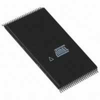
AT49BV802AT-70TU Atmel, AT49BV802AT-70TU Datasheet - Page 22

AT49BV802AT-70TU
Manufacturer Part Number
AT49BV802AT-70TU
Description
IC FLASH 8MBIT 70NS 48TSOP
Manufacturer
Atmel
Datasheet
1.AT49BV802A-70TU.pdf
(31 pages)
Specifications of AT49BV802AT-70TU
Format - Memory
FLASH
Memory Type
FLASH
Memory Size
8M (1M x 8 or 512K x 16)
Speed
70ns
Interface
Parallel
Voltage - Supply
2.65 V ~ 3.6 V
Operating Temperature
-40°C ~ 85°C
Package / Case
48-TSOP
Lead Free Status / RoHS Status
Lead free / RoHS Compliant
Available stocks
Company
Part Number
Manufacturer
Quantity
Price
21. Program Cycle Characteristics
22. Program Cycle Waveforms
23. Sector or Chip Erase Cycle Waveforms
Notes:
22
Symbol
t
t
t
t
t
t
t
t
t
t
t
t
t
t
BP
AS
AH
DS
DH
WP
WPH
WC
RP
EC
SEC1
SEC2
ES
PS
1. OE must be high only when WE and CE are both low.
2. For chip erase, the address should be 555. For sector erase, the address depends on what sector is to be erased.
3. For chip erase, the data should be 10H, and for sector erase, the data should be 30H.
AT49BV802A(T)
(See note 3 under
Parameter
Byte/Word Programming Time
Address Setup Time
Address Hold Time
Data Setup Time
Data Hold Time
Write Pulse Width
Write Pulse Width High
Write Cycle Time
Reset Pulse Width
Chip Erase Cycle Time
Sector Erase Cycle Time (4K Word Sectors)
Sector Erase Cycle Time (32K Word Sectors)
Erase Suspend Time
Program Suspend Time
A0-A18
“Command Definition Table” on page
DATA
WE
OE
CE
A0 - A18
(1)
DATA
WE
OE
CE
t
AS
t
AS
555
t
WC
WORD 0
t
AH
AA
555
t
WC
t
AH
t
t
DS
WP
AA
AAA
t
t
DS
WP
WORD 1
t
DH
AAA
55
t
DH
55
555
t
WPH
WORD 2
555
80
PROGRAM CYCLE
t
WPH
13.)
A0
555
WORD 3
ADDRESS
AA
INPUT
DATA
AAA
WORD 4
55
Min
500
35
35
35
35
70
t
0
0
BP
Note 2
WORD 5
Note 3
555
t
EC
AA
Typ
0.3
1.0
12
13
Max
200
3.0
5.0
15
10
3405E–FLASH–2/07
seconds
seconds
seconds
Units
µs
ns
ns
ns
ns
ns
ns
ns
ns
µs
µs


