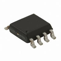
W25P16VSSIG Winbond Electronics, W25P16VSSIG Datasheet - Page 9

W25P16VSSIG
Manufacturer Part Number
W25P16VSSIG
Description
IC FLASH 16MBIT 50MHZ 8SOIC
Manufacturer
Winbond Electronics
Datasheet
1.W25P16VSFIG.pdf
(43 pages)
Specifications of W25P16VSSIG
Format - Memory
FLASH
Memory Type
FLASH
Memory Size
16M (2M x 8)
Speed
50MHz
Interface
SPI Serial
Voltage - Supply
2.7 V ~ 3.6 V
Operating Temperature
-40°C ~ 85°C
Package / Case
8-SOIC
Lead Free Status / RoHS Status
Lead free / RoHS Compliant
Available stocks
Company
Part Number
Manufacturer
Quantity
Price
Company:
Part Number:
W25P16VSSIG
Manufacturer:
MICONAS
Quantity:
567
8. FUNCTIONAL DESCRIPTION
8.1
8.1.1
The W25P80/16 is accessed through an SPI compatible bus consisting of four signals: Serial Clock
(CLK), Chip Select (/CS), Serial Data Input (DI) and Serial Data Output (DO). Both SPI bus operation
Modes 0 (0,0) and 3 (1,1) are supported. The primary difference between Mode 0 and Mode 3
concerns the normal state of the CLK signal when the SPI bus master is in standby and data is not
being transferred to the Serial Flash. For Mode 0 the CLK signal is normally low. For Mode 3 the CLK
signal is normally high. In either case data input on the DI pin is sampled on the rising edge of the
CLK. Data output on the DO pin is clocked out on the falling edge of CLK.
8.1.2
The /HOLD signal allows the W25P80/16 operation to be paused while it is actively selected (when
/CS is low). The /HOLD function may be useful in cases where the SPI data and clock signals are
shared with other devices. For example, consider if the page buffer was only partially written when a
priority interrupt requires use of the SPI bus. In this case the /HOLD function can save the state of the
instruction and the data in the buffer so programming can resume where it left off once the bus is
available again.
To initiate a /HOLD condition, the device must be selected with /CS low. A /HOLD condition will
activate on the falling edge of the /HOLD signal if the CLK signal is already low. If the CLK is not
already low the /HOLD condition will activate after the next falling edge of CLK. The /HOLD condition
will terminate on the rising edge of the /HOLD signal if the CLK signal is already low. If the CLK is not
already low the /HOLD condition will terminate after the next falling edge of CLK.
During a /HOLD condition, the Serial Data Output (DO) is high impedance, and Serial Data Input (DI)
and Serial Clock (CLK) are ignored. The Chip Select (/CS) signal should be kept active (low) for the
full duration of the /HOLD operation to avoid resetting the internal logic state of the device.
8.2
Applications that use non-volatile memory must take into consideration the possibility of noise and
other adverse system conditions that may compromise data integrity. To address this concern the
W25P80/16 provides several means to protect data from inadvertent writes.
8.2.1
• Device resets when VCC is below threshold.
• Time delay write disable after Power-up.
• Write enable/disable instructions.
• Automatic write disable after program and erase.
• Software write protection using Status Register.
• Hardware write protection using Status Register and /WP pin.
• Write Protection using Power-down instruction.
SPI OPERATIONS
WRITE PROTECTION
SPI Modes
HOLD Function
Write Protect Features
- 9 -
W25P80 AND W25P16
Publication Release Date: January 19, 2007
Revision M


