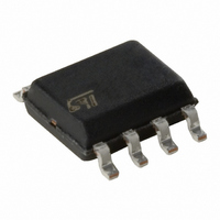
M24128-BWMN6P STMicroelectronics, M24128-BWMN6P Datasheet - Page 24

M24128-BWMN6P
Manufacturer Part Number
M24128-BWMN6P
Description
IC EEPROM 128KBIT 400KHZ 8SOIC
Manufacturer
STMicroelectronics
Specifications of M24128-BWMN6P
Format - Memory
EEPROMs - Serial
Memory Type
EEPROM
Memory Size
128K (16K x 8)
Speed
400kHz
Interface
I²C, 2-Wire Serial
Voltage - Supply
2.5 V ~ 5.5 V
Operating Temperature
-40°C ~ 85°C
Package / Case
8-SOIC (3.9mm Width)
Organization
16 K x 8
Interface Type
I2C
Maximum Clock Frequency
0.4 MHz
Access Time
900 ns
Supply Voltage (max)
5.5 V
Supply Voltage (min)
2.5 V
Maximum Operating Current
2 mA
Maximum Operating Temperature
+ 85 C
Mounting Style
SMD/SMT
Minimum Operating Temperature
- 40 C
Operating Supply Voltage
2.5 V, 5.5 V
Memory Configuration
16384 X 8
Clock Frequency
400kHz
Supply Voltage Range
2.5V To 5.5V
Memory Case Style
SO
No. Of Pins
8
Rohs Compliant
Yes
Lead Free Status / RoHS Status
Lead free / RoHS Compliant
Other names
497-8577-5
M24128-BWMN6P
M24128-BWMN6P
Available stocks
Company
Part Number
Manufacturer
Quantity
Price
Company:
Part Number:
M24128-BWMN6P
Manufacturer:
STMicroelectronics
Quantity:
1 885
Company:
Part Number:
M24128-BWMN6P
Manufacturer:
STMicroelectronics
Quantity:
3 050
Part Number:
M24128-BWMN6P
Manufacturer:
STM专家
Quantity:
20 000
DC and AC parameters
Table 13.
1. Characterized value, not tested in production.
2. The device is not selected after power-up, after a Read command (after the Stop condition) or after the completion of the
Table 14.
1. If the application uses the M24128-BR at 2.5 V < V
2. Characterized value, not tested in production.
3. The device is not selected after power-up, after a Read command (after the Stop condition) or after the completion of the
24/39
Symbol
Symbol
I
I
V
internal write cycle t
I
V
characteristics (M24xxx-W, device grade 6)
internal write cycle t
I
I
I
CC0
CC1
V
V
I
I
V
LO
CC
I
CC0
CC1
V
OL
I
LI
CC
LO
IH
IL
OL
LI
IH
IL
Input leakage current
(SCL, SDA, E2, E1, E0)
Output leakage current
Supply current (Read)
Supply current (Write)
Standby supply current
Input low voltage (SDA, SCL, WC)
Input high voltage (SCL, SDA)
Input high voltage (WC, E0, E1, E2)
Output low voltage
Input leakage current (SCL, SDA,
E2, E1, E0)
Output leakage current
Supply current (Read)
Supply current (Write)
Standby supply current
Input low voltage (SDA, SCL, WC)
Input high voltage (SCL, SDA)
Input high voltage (WC, E0, E1, E2)
Output low voltage
DC characteristics (M24xxx-W, device grade 3)
DC characteristics (M24xxx-R - device grade 6)
W
W
(t
(t
Parameter
W
W
Parameter
is triggered by the correct decoding of a Write command).
is triggered by the correct decoding of a Write command).
instead of the above table.
Doc ID 16892 Rev 19
Device not selected
CC
Test condition (in addition to
During t
Device not selected
2.5 V < V
(in addition to those in
applied on SDA: V
< 5.5 V and –40 °C < T
SDA Hi-Z, external voltage
During t
V
device in Standby mode
I
SDA in Hi-Z, external voltage
I
OL
applied on SDA: V
OL
CC
V
those in
or V
1.8 V V
2.5 V V
device in Standby mode
I
OL
CC
V
= 1 mA, V
= 2.1 mA, V
= 1.8 V, f
W
IN
V
, 2.5 V < V
= 3 mA, V
, 1.8 V < V
CC
Test condition
CC
W
= V
IN
, V
, 2.5 V < V
= V
< 5.5 V, f
SS
Table
CC
CC
CC
c
SS
CC
or V
= 400 kHz
= 1.8 V
< 2.5 V
< 5.5 V
(3)
CC
CC
or V
(2)
SS
CC
= 1.8 V
CC
, V
8)
CC
, V
M24128-BW, M24128-BR, M24128-BF
A
SS
= 2.5 V or
or V
c
CC
= 5.5 V
(1)
< 5.5 V
< 2.5 V
IN
CC
< +85 °C, please refer to
= 400 kHz
IN
or V
< 5.5 V
= V
Table
= V
CC
CC
SS
SS
7)
or
0.7V
0.7V
–0.45
–0.45
Min.
0.7V
0.7V
–0.45
Min.
CC
CC
CC
CC
0.25 V
Table 12: DC
V
0.3 V
V
0.3V
CC
Max.
CC
3
Max.
± 2
± 2
0.8
6.5
0.2
5
± 2
± 2
6.5
0.4
1
(2)
10
+0.6
2
(1)
+0.6
CC
CC
CC
Unit
Unit
mA
mA
mA
mA
µA
µA
µA
µA
µA
µA
V
V
V
V
V
V
V
V
V


