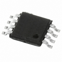
M93C46-RDS6G STMicroelectronics, M93C46-RDS6G Datasheet - Page 10

M93C46-RDS6G
Manufacturer Part Number
M93C46-RDS6G
Description
IC EEPROM 1KBIT 1MHZ 8TSSOP
Manufacturer
STMicroelectronics
Datasheet
1.M93C46-RDS6G.pdf
(30 pages)
Specifications of M93C46-RDS6G
Format - Memory
EEPROMs - Serial
Memory Type
EEPROM
Memory Size
1K (128 x 8 or 64 x 16)
Speed
1MHz
Interface
Microwire, 3-Wire Serial
Voltage - Supply
1.8 V ~ 5.5 V
Operating Temperature
-40°C ~ 85°C
Package / Case
8-TSSOP
Lead Free Status / RoHS Status
Lead free / RoHS Compliant
M93C86, M93C76, M93C66, M93C56, M93C46, M93C06
Figure 7. WRAL Sequence
Note: For the meanings of Xn and Dn, please see Table 4, Table 5 and Table 6.
Write All
As with the Erase All Memory (ERAL) instruction,
the format of the Write All Memory with same Data
(WRAL) instruction requires that a dummy ad-
dress be provided. As with the Write Data to Mem-
ory (WRITE) instruction, the format of the Write All
Memory with same Data (WRAL) instruction re-
quires that an 8-bit data byte, or 16-bit data word,
be provided. This value is written to all the ad-
dresses of the memory device. The completion of
the cycle can be detected by monitoring the
Ready/Busy line, as described next.
READY/BUSY STATUS
While the Write or Erase cycle is underway, for a
WRITE, ERASE, WRAL or ERAL instruction, the
Busy signal (Q=0) is returned whenever Chip Se-
lect Input (S) is driven High. (Please note, though,
that there is an initial delay, of t
10/30
WRITE
ALL
S
Q
D
1
CODE
0
OP
SLSH
0 0
1 Xn X0
ADDR
, before this
Dn
DATA IN
status information becomes available). In this
state, the M93Cx6 ignores any data on the bus.
When the Write cycle is completed, and Chip Se-
lect Input (S) is driven High, the Ready signal
(Q=1) indicates that the M93Cx6 is ready to re-
ceive the next instruction. Serial Data Output (Q)
remains set to 1 until the Chip Select Input (S) is
brought Low or until a new start bit is decoded.
COMMON I/O OPERATION
Serial Data Output (Q) and Serial Data Input (D)
can be connected together, through a current lim-
iting resistor, to form a common, single-wire data
bus. Some precautions must be taken when oper-
ating the memory in this way, mostly to prevent a
short circuit current from flowing when the last ad-
dress bit (A0) clashes with the first data bit on Se-
rial Data Output (Q). Please see the application
note AN394 for details.
D0
BUSY
STATUS
CHECK
READY
AI00880C


