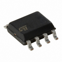
M93S66-WMN6P STMicroelectronics, M93S66-WMN6P Datasheet

M93S66-WMN6P
Specifications of M93S66-WMN6P
M93S66-WMN6P
Related parts for M93S66-WMN6P
M93S66-WMN6P Summary of contents
Page 1
... Clock Rate, 5ms Write Time (New Product, identified by process identification letter Sequential Read Operation Enhanced ESD/Latch-Up Behavior More than 1 Million Erase/Write Cycles More than 40 Year Data Retention M93S66, M93S56 4Kbit, 2Kbit and 1Kbit (16-bit wide) Figure 1. Packages 8 PDIP8 (BN) 8 SO8 (MN) ...
Page 2
... High, the M93Sx6 can output a sequential stream of data words. In this way, the memory can be read as a data stream from 16 to 4096 bits (for the M93S66), or continuously as the address counter automatically rolls over to 00h when the highest address is reached. Within the time required by a programming cycle ...
Page 3
... The address bits of the byte or word that is to 6.. be accessed. For the M93S46, the address is made bits (see M93S56 and M93S66, the address is made bits (see The M93Sx6 devices are fabricated in CMOS technology and are therefore able to run as slow (static input signals fast as the max- ...
Page 4
... M93S66, M93S56, M93S46 MAXIMUM RATING Stressing the device above the rating listed in the Absolute Maximum Ratings" table may cause per- manent damage to the device. These are stress ratings only and operation of the device at these or any other conditions above those indicated in the Operating sections of this specification is not im- Table 4 ...
Page 5
... Conditions summarized in the relevant tables. Designers should check that the operating conditions in their circuit match the measurement conditions when relying on the quoted parame- ters. Parameter Parameter Parameter Parameter Parameter M93S66, M93S56, M93S46 Min. Max. Unit 4.5 5.5 V –40 85 °C –40 125 ° ...
Page 6
... M93S66, M93S56, M93S46 Figure 9. AC Testing Input Output Waveforms 0.8V CC 0.2V CC Table 10. Capacitance Symbol Parameter C Output OUT Capacitance C Input IN Capacitance Note: Sampled only, not 100% tested 18/34 M93SXX 2. 0.4V INPUT OUTPUT M93SXX-W & M93SXX-R Test Condition OUT =25°C and a frequency of 1 MHz. ...
Page 7
... M93S66, M93S56, M93S46 Table 13. DC Characteristics (M93Sx6-W, Device Grade 6) Symbol Parameter I Input Leakage Current LI I Output Leakage Current LO Supply Current (CMOS I CC Inputs) I Supply Current (Stand-by) CC1 V Input Low Voltage ( Input High Voltage ( Output Low Voltage ( Output High Voltage (Q) OH Note: 1. Current product: identified by Process Identification letter ...
Page 8
... Supply Current (Stand-by) CC1 V Input Low Voltage ( Input High Voltage ( Output Low Voltage ( Output High Voltage (Q) OH Note: 1. Preliminary Data: this product is under development. For more infomation, please contact your nearest ST sales office. M93S66, M93S56, M93S46 Test Condition Hi-Z OUT 5V MHz ...
Page 9
... Chip Select Input (S) must be brought Low for a minimum of tSLSH between consecutive instruction cycles. 3. Current product: identified by Process Identification letter New product: identified by Process Identification letter Table 9. 3 Parameter Min. D. 250 250 100 1000 350 250 100 100 100 0 M93S66, M93S56, M93S46 and Table Max. Min. Max 250 50 50 200 200 200 ...
Page 10
... M93S66, M93S56, M93S46 Table 18. AC Characteristics (M93Sx6-W, Device Grade 3) Test conditions specified in Symbol Alt Clock Frequency Protect Enable Valid to Clock High PRVCH PRES t t Write Enable Valid to Clock High WVCH PES t t Clock Low to Protect Enable Transition CLPRX PREH t t Chip Select Low to Write Enable Transition ...
Page 11
... M93S66, M93S56, M93S46 h x 45˚ inches Typ. Min. 0.053 0.004 0.013 0.007 0.189 0.150 0.050 – 0.228 0.010 0.016 0° 8 Max. ...
Page 12
... M93S66, M93S56, M93S46 PART NUMBERING Table 24. Ordering Information Scheme Example: Device Type M93 = MICROWIRE serial access EEPROM (x16) with Block Protection Device Function Kbit (256 x 16 Kbit (128 x 16 Kbit (64 x 16) Operating Voltage blank = V = 4 2 1.8 to 5.5V CC Package ...


