AT17C256-10JC Atmel, AT17C256-10JC Datasheet - Page 4
AT17C256-10JC
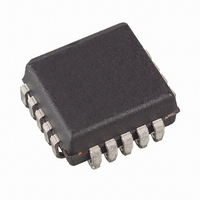
Manufacturer Part Number
AT17C256-10JC
Description
IC SER CONFIG PROM 256K 20PLCC
Manufacturer
Atmel
Datasheet
1.AT17C128-10JC.pdf
(14 pages)
Specifications of AT17C256-10JC
Programmable Type
Serial EEPROM
Memory Size
256Kb
Voltage - Supply
4.75 V ~ 5.25 V
Operating Temperature
0°C ~ 70°C
Package / Case
20-LCC (J-Lead)
Lead Free Status / RoHS Status
Contains lead / RoHS non-compliant
Available stocks
Company
Part Number
Manufacturer
Quantity
Price
Company:

Part Number:
AT17C256-10JC
Manufacturer:
ATM
Quantity:
5 704
Company:
Part Number:
AT17C256-10JC
Manufacturer:
ATM
Quantity:
5 704
Company:
Part Number:
AT17C256-10JC
Manufacturer:
ATM
Quantity:
6 100
Part Number:
AT17C256-10JC
Manufacturer:
AT
Quantity:
20 000


Pin Configurations
Absolute Maximum Ratings*
4
Operating Temperature.................................. -55°C to +125°C
Storage Temperature ..................................... -65°C to +150°C
Voltage on Any Pin
with Respect to Ground ..............................-0.1V to V
Supply Voltage (V
Maximum Soldering Temp. (10 sec. @ 1/16 in.).............260°C
ESD (R
PLCC/
SOIC
Pin
20
10
14
17
20
2
4
6
8
ZAP
= 1.5K, C
SOIC
DIP/
Pin
8
1
2
3
4
5
6
7
8
CC
AT17C/LV65/128/256
) .........................................-0.5V to +7.0V
ZAP
RESET/OE
= 100pF).................................. 2000V
SER_EN
Name
DATA
GND
CEO
VCC
CLK
WP
CE
A2
I/O
I/O
O
I
I
I
I
I
I
Description
Three-state DATA output for configuration. Open-collector bi-directional pin for
programming.
Clock input. Used to increment the internal address and bit counter for reading and
programming.
RESET/Output Enable input (when SER_EN is High). A Low level on both the CE and
RESET/OE inputs enables the data output driver. A High level on RESET/OE resets
both the address and bit counters. The logic polarity of this input is programmable as
either RESET/OE or RESET/OE. This document describes the pin as RESET/OE.
Write protect (WP) input (when CE is Low). When WP is Low, the entire memory can
be written. When WP is enabled (High), the lowest block of the memory cannot be
written. This feature is only active in the 2-wire serial Programming Mode (i.e., when
SER_EN is Low; see “Programming Specification” application note for more details).
Chip Enable input. Used for device selection. A Low level on both CE and OE enables
the data output driver. A High level on CE disables both the address and bit counters
and forces the device into a low-power standby mode. Note that this pin will not
enable/disable the device in the 2-wire Serial Programming Mode (i.e., when SER_EN
is Low).
Ground pin. A 0.2 µF decoupling capacitor between VCC and GND is recommended.
Chip Enable Output. This signal is asserted Low on the clock cycle following the last bit
read from the memory. It will stay Low as long as CE and OE are both Low. It will then
follow CE until OE goes High. Thereafter, CEO will stay High until the entire EEPROM
is read again.
Device selection input, A2. This is used to enable (or select) the device during
programming (i.e. when SER_EN is Low; see the “Programming Specification”
application note for more details.
Serial enable must be held High during FPGA loading operations. Bringing SER_EN
Low enables the 2-wire Serial Programming Mode.
+3.3V/+5V Power Supply Pin.
CC
+0.5V
*NOTICE:
Stresses beyond those listed under Absolute
Maximum Ratings may cause permanent dam-
age to the device. This is a stress rating only and
functional operation of the device at these or any
other conditions beyond those listed under oper-
ating conditions is not implied. Exposure to Abso-
lute Maximum Rating conditions for extended
periods of time may affect device reliability.
Related parts for AT17C256-10JC
Image
Part Number
Description
Manufacturer
Datasheet
Request
R

Part Number:
Description:
Manufacturer:
ATMEL Corporation
Datasheet:

Part Number:
Description:
IC SERIAL CONFIG PROM 256K 8DIP
Manufacturer:
Atmel
Datasheet:

Part Number:
Description:
IC SER CONFIG PROM 256K 20PLCC
Manufacturer:
Atmel
Datasheet:

Part Number:
Description:
IC EEPROM FPGA 256KB 20-SOIC
Manufacturer:
Atmel
Datasheet:
Part Number:
Description:
IC EEPROM FPGA 256KB 20-SOIC
Manufacturer:
Atmel
Datasheet:

Part Number:
Description:
IC EEPROM FPGA 256KB 8-SOIC
Manufacturer:
Atmel
Datasheet:
Part Number:
Description:
IC EEPROM FPGA 256KB 8-SOIC
Manufacturer:
Atmel
Datasheet:
Part Number:
Description:
IC SERIAL CONFIG PROM 256K 8-DIP
Manufacturer:
Atmel
Datasheet:


Part Number:
Description:
DEV KIT FOR AVR/AVR32
Manufacturer:
Atmel
Datasheet:
Part Number:
Description:
INTERVAL AND WIPE/WASH WIPER CONTROL IC WITH DELAY
Manufacturer:
ATMEL Corporation
Datasheet:
Part Number:
Description:
Low-Voltage Voice-Switched IC for Hands-Free Operation
Manufacturer:
ATMEL Corporation
Datasheet:
Part Number:
Description:
MONOLITHIC INTEGRATED FEATUREPHONE CIRCUIT
Manufacturer:
ATMEL Corporation
Datasheet: