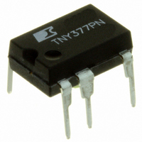
TNY377PN Power Integrations, TNY377PN Datasheet - Page 7

TNY377PN
Manufacturer Part Number
TNY377PN
Description
IC OFFLINE SWIT OVP OTP HV 8DIP
Manufacturer
Power Integrations
Series
TinySwitch®-PKr
Type
Off Line Switcherr
Datasheet
1.TNY376PN.pdf
(22 pages)
Specifications of TNY377PN
Output Isolation
Isolated
Frequency Range
132 ~ 280kHz
Voltage - Output
700V
Power (watts)
28W
Operating Temperature
-40°C ~ 150°C
Package / Case
8-DIP (0.300", 7.62mm), 7 Leads
Output Voltage
700 V
Input / Supply Voltage (max)
9 V
Input / Supply Voltage (min)
- 0.3 V
Duty Cycle (max)
65 %
Switching Frequency
264 KHz
Supply Current
570 uA
Operating Temperature Range
- 40 C to + 150 C
Mounting Style
Through Hole
Maximum Operating Temperature
+ 150 C
Minimum Operating Temperature
- 40 C
Output Current
1.4 A
Output Power
28 W
Lead Free Status / RoHS Status
Lead free / RoHS Compliant
Other names
596-1144-5
Available stocks
Company
Part Number
Manufacturer
Quantity
Price
Company:
Part Number:
TNY377PN
Manufacturer:
POWER
Quantity:
15 000
reduced, and the clock frequency is reduced to half that at the
highest current limit level (Figure 8). At very light loads, the
current limit will be reduced even further (Figure 9). Only a small
percentage of cycles will occur to satisfy the power consumption
of the power supply. The response time of the ON/OFF control
scheme is very fast compared to PWM control. This provides
tight regulation and excellent transient response.
Power Up/Down
The TinySwitch-PK requires only a 0.1 μF capacitor on the
BYPASS/MULTI-FUNCTION pin to operate with standard
current limit. Because of its small size, the time to charge this
capacitor is kept to an absolute minimum, typically 0.6 ms. The
time to charge will vary in proportion to the BYPASS/MULTI-
FUNCTION pin capacitor value when selecting different current
limits. Due to the high bandwidth of the ON/OFF feedback,
there is no overshoot at the power supply output. When an
external resistor (4 MΩ) is connected from the power supply
positive DC input to the EN/UV pin, the power MOSFET
switching will be delayed during power-up until the DC line
voltage exceeds the threshold (100 V). Figures 10 and 11 show
the power-up timing waveform in applications with and without
an external resistor (4 MΩ) connected to the EN/UV pin.
During power-down, when an external resistor is used, the
power MOSFET will switch for 32 ms after the output loses
regulation. The power MOSFET will then remain off without any
glitches since the undervoltage function prohibits restart when
the line voltage is low.
Figure 12 illustrates a typical power-down timing waveform.
Figure 13 illustrates a very slow power-down timing waveform,
as in standby applications. The external resistor (4 MΩ) is
connected to the EN/UV pin in this case to prevent unwanted
restarts.
www.powerint.com
With the TNY375 and TNY376, no bias winding is needed to
provide power to the chip because it draws the power directly
from the DRAIN pin (see Functional Description above). This
eliminates the cost of a bias winding and associated
components. For the TNY377-380 or for applications that require
very low no-load power consumption (50 mW), a resistor from a
bias winding to the BYPASS/MULTI-FUNCTION pin can provide
the power to the chip. The minimum recommended current
supplied is I
case will be clamped at 6.4 V. This method will eliminate the
power draw from the DRAIN pin, thereby reducing the no-load
power consumption and improving full-load effi ciency.
Current Limit Operation
Each switching cycle is terminated when the DRAIN current
reaches the current limit of the device. Current limit operation
provides good line ripple rejection and relatively constant power
delivery independent of input voltage.
BYPASS/MULTI-FUNCTION Pin Capacitor
The BYPASS/MULTI-FUNCTION pin can use a ceramic
capacitor as small as 0.1 μF for decoupling the internal power
supply of the device. A larger capacitor size can be used to
adjust the current limit. A 1 μF BP/M pin capacitor will select a
lower current limit equal to the standard current limit of the next
smaller device, and a 10 μF BP/M pin capacitor will select a
higher current limit equal to the standard current limit of the next
larger device. The TNY375 and TNY376 MOSFETs do not have
the capability to match the current limit of the next larger
devices in the family. The current limit is therefore increased to
the maximum capability of their respective MOSFETs. The
higher current limit level of the TNY380 is set to 1105 mA typical.
The smaller current limit of the TNY375 is set to 325 mA.
S2
+ I
DIS
. The BYPASS/MULTI-FUNCTION pin in this
TNY375-380
Rev. C 07/09
7


