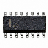
MC33363ADW ON Semiconductor, MC33363ADW Datasheet - Page 11

MC33363ADW
Manufacturer Part Number
MC33363ADW
Description
IC SWIT PROG OVP UVLO HV 16SOIC
Manufacturer
ON Semiconductor
Type
High Voltage Switching Regulatorr
Datasheet
1.MC33363ADWR2G.pdf
(13 pages)
Specifications of MC33363ADW
Output Isolation
Isolated
Frequency Range
59 ~ 315kHz
Voltage - Input
9.5 ~ 40 V
Voltage - Output
700V
Operating Temperature
-25°C ~ 150°C
Package / Case
16-SOIC (0.300", 7.50mm Width) 13 leads
Output Voltage Range
5.5 V to 7.5 V
Input Voltage Range
40 V
Mounting Style
SMD/SMT
Lead Free Status / RoHS Status
Contains lead / RoHS non-compliant
Available stocks
Company
Part Number
Manufacturer
Quantity
Price
Company:
Part Number:
MC33363ADW
Manufacturer:
ON
Quantity:
5 510
Part Number:
MC33363ADW
Manufacturer:
MOTOROLA/摩托罗拉
Quantity:
20 000
Company:
Part Number:
MC33363ADWG
Manufacturer:
ON Semiconductor
Quantity:
20
Part Number:
MC33363ADWR2G
Manufacturer:
ON/安森美
Quantity:
20 000
92 to 276
1200 pF
Vac Input
13 k
1.0
C4
C3
R1
1.0 A
8
6
7
F1
Table 1. CONVERTER TEST DATA
*With MBR2535CTL, 78.8% efficiency. PCB layout modification is required to use this rectifier.
Line Regulation
Load Regulation
Output Ripple
Efficiency
This data was taken with the components listed below mounted on the printed circuit board shown in Figure 23.
For high efficiency and small circuit board size, the Sanyo Os--Con capacitors are recommended for C8, C9, C10
and C11.
C8, C9, C10 = Sanyo Os--Con #6SA330M, 330 mF 6.3 V.
C11 = Sanyo Os--Con #10SA220M, 220 mF 10 V.
L1 = Coilcraft S5088--A, 5.0 mH, 0.11 Ω.
T1 = Coilcraft U6875--A
D4
D2
Primary: 77 turns of # 28 AWG, Pin 1 = start, Pin 8 = finish.
Two layers 0.002 Mylar tape.
Secondary: 5 turns of # 22 AWG, 2 strands bifiliar wound, Pin 5 = start, Pin 4 = finish.
Two layers 0.002 Mylar tape.
Auxiliary: 13 turns of # 28 AWG wound in center of bobbin, Pin 2 = start, Pin 7 = finish.
Two layers 0.002 Mylar tape.
Gap: 0.011 total for a primary inductance (L
Core and Bobbin: Coilcraft PT1950, E187, 3F3 material.
Mirror
Thermal
Test
D1
D3
PWM
Osc
1N4006
V
V
V
V
V
V
V
4, 5, 12, 13
in
in
in
in
in
in
in
Reg
= 92 Vac to 276 Vac, I
= 115 Vac, I
= 230 Vac, I
= 115 Vac, I
= 230 Vac, I
= 115 Vac, I
= 230 Vac, I
PWM Latch
270 A
C1
47
S
R
I Limit
Conditions
Figure 22. 15 W Off- -Line Converter
Q
O
O
O
Startup
O
O
O
= 0.75 A to 3.0 A
= 3.0 A
= 3.0 A
= 0.75 A to 3.0 A
= 3.0 A
= 3.0 A
Driver
EA
LEB
http://onsemi.com
O
P
) of 620 mH.
3.0 A
IC1 MC33363A
14.5 V/
9.5 V
2.6 V
UVLO
OVP
1
2.6 V
11
4.0 nF
10
C5
11
16
9
3
Δ = 5.0 mV
Triangular = 2.0 mVpp, Spike = 34 mVpp
76.8%
Δ = 1.0 mV
Δ = 5.0 mV
Triangular = 2.0 mVpp, Spike = 32 mVpp
76.8%*
R2
2.7 k
R4
5.1 k
R3
1.0 k
1100E
C2
10
1.0 W
180 k
MUR
5
4
D5
R6
R5
39
MUR
C6
47 pF
R7
2.2 k
1.0 W
120
D6
Results
T1
MBR
1635
D7
330
MOC
8103
C8
IC2
TL431B
330
C9
IC3
330
C10
1
2
3
2
5.0 H
100 nF
R8
220
2.80 k
C7
L1
1
2.74 k
R9
R10
5.05 V/3.0 A
DC Output
C11
220
C12
1.0
+
--


