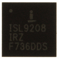
ISL9208IRZ Intersil, ISL9208IRZ Datasheet - Page 23

ISL9208IRZ
Manufacturer Part Number
ISL9208IRZ
Description
IC MULTI-CELL LI-ION PROT 32-QFN
Manufacturer
Intersil
Specifications of ISL9208IRZ
Function
Battery Monitor
Battery Type
Lithium-Ion (Li-Ion)
Voltage - Supply
5 V ~ 10 V
Operating Temperature
-40°C ~ 85°C
Mounting Type
Surface Mount
Package / Case
32-VQFN Exposed Pad, 32-HVQFN, 32-SQFN, 32-DHVQFN
Interface Type
I2C, Serial
Battery Protection
Over Current
No. Of Batteries
7
Supply Voltage Range
9.2V To 30.1V
Battery Ic Case Style
QFN
No. Of Pins
32
Rohs Compliant
Yes
Operating Temperature Range
-40°C To +85°C
Ic Interface Type
I2C
Lead Free Status / RoHS Status
Lead free / RoHS Compliant
Available stocks
Company
Part Number
Manufacturer
Quantity
Price
Company:
Part Number:
ISL9208IRZ
Manufacturer:
Intersil
Quantity:
500
Part Number:
ISL9208IRZ
Manufacturer:
INTERSIL
Quantity:
20 000
Company:
Part Number:
ISL9208IRZ-T
Manufacturer:
OSRAM
Quantity:
2 506
WRITE OPERATIONS
For a write operation, the device requires a slave byte and
an address byte. The slave byte specifies the particular
device on the I
address specifies one of the registers in that device. After
receipt of each byte, the device responds with an
acknowledge, and awaits the next eight bits from the master.
After the acknowledge, following the transfer of data, the
master terminates the transfer by generating a stop
condition. See Figure 12.
When receiving data from the master, the value in the data
byte is transferred into the register specified by the address
byte on the falling edge of the clock following the 8th data bit.
After receiving the acknowledge after the data byte, the
device automatically increments the address. So, before
sending the stop bit, the master may send additional data to
the device without re-sending the slave and address bytes.
After writing to address 0AH, the address “wraps around” to
address 0. Do not continue to write to addresses higher than
address 08H, since these addresses access registers that
are reserved. Writing to these locations can result in
unexpected device operation.
SDA BUS
SDA BUS
A
R
S
T
T
A
R
0 1 0 1
S
T
T
2
0 1 0 1
FIGURE 12. WRITE SEQUENCE
SLAVE
C bus that the master is writing to. The
BYTE
SLAVE
BYTE
0
0 0
0
ISL9208: SLAVE BYTE = 50H
0 0
0
A
C
K
0
A
C
K
23
REGISTER
ADDRESS
Random Read
REGISTER
ADDRESS
A
C
K
A
C
K
S
A
R
T
T
DATA
0 1 0 1
FIGURE 13. READ SEQUENCE
SLAVE
BYTE
0
0 0
ISL9208: SLAVE BYTE = 010100xH
A
C
K
O
S
T
P
1
ISL9208
A
C
K
DATA
Read Operations
Read operations are initiated in the same manner as write
operations with the host sending the address where the read
is to start (but no data). Then, the host sends an ACK, a
repeated start, and the slave byte with the LSB=1. After the
device acknowledges the slave byte, the device sends out
one bit of data for each master clock. After the slave sends
eight bits to the master, the master sends a NACK (Not
acknowledge) to the device, to indicate the data transfer is
complete, then the master sends a stop bit. See Figure 13.
After sending the eighth data bit to the master, the device
automatically increments its internal address pointer. So the
master, instead of sending a NACK and the stop bit, can
send additional clocks to read the contents of the next
register - without sending another slave and address byte.
If the last address read or written is known, the master can
initiate a current address read. In this case, only the slave
byte is sent before data is returned. (See Figure 13.)
.
N
A
C
K
S
O
P
T
S
T
A
R
T
Current Address Read
0 1 0 1
SLAVE
BYTE
0
0 0
1
A
C
K
DATA
November 2, 2007
FN6446.1
N
A
C
K
O
S
T
P


