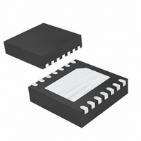
DS2741N+T Maxim Integrated Products, DS2741N+T Datasheet - Page 8

DS2741N+T
Manufacturer Part Number
DS2741N+T
Description
IC MONITOR/ACCUMULATOR 14-TDFN
Manufacturer
Maxim Integrated Products
Datasheet
1.DS2741NT.pdf
(10 pages)
Specifications of DS2741N+T
Function
Fuel, Gas Gauge/Monitor
Battery Type
Lithium-Ion (Li-Ion)
Voltage - Supply
2.5 V ~ 4.5 V
Operating Temperature
-20°C ~ 70°C
Mounting Type
Surface Mount
Package / Case
14-WFDFN Exposed Pad
Lead Free Status / RoHS Status
Lead free / RoHS Compliant
Current Monitor and Accumulator with
Integrated Sense Resistor
8
Bit Read: At the end a write operation, the master
must release the SDA bus line for the proper amount
of setup time (Figure 4) before the next rising edge
of SCL during a bit read. The device shifts out each
bit of data on SDA at the falling edge of the previous
SCL pulse, and the data bit is valid at the rising
edge of the current SCL pulse. Remember that the
master generates all SCL clock pulses, including
when it is reading bits from the slave.
Acknowledgement (ACK and NACK): An acknowl-
edgement (ACK) or not acknowledge (NACK) is
always the 9th bit transmitted during a byte transfer.
The device receiving data (the master during a read
or the slave during a write operation) performs an
ACK by transmitting a zero during the 9th bit. A
device performs a NACK by transmitting a one dur-
ing the 9th bit. Timing for the ACK and NACK is
identical to all other bit writes (see Figure 4). An
ACK is the acknowledgment that the device is prop-
erly receiving data. A NACK is used to terminate a
read sequence or as an indication that the device is
not receiving data.
Byte Write: A byte write consists of 8 bits of infor-
mation transferred from the master to the slave
(most significant bit first) plus a 1-bit acknowledge-
ment from the slave to the master. The 8 bits trans-
mitted by the master are done according to the
bit-write definition and the acknowledgement is read
using the bit-read definition.
Byte Read: A byte read is an 8-bit information trans-
fer from the slave to the master plus a 1-bit ACK or
NACK from the master to the slave. The 8 bits of
information that are transferred (most significant bit
first) from the slave to the master are read by the
master using the bit-read definition, and the master
transmits an ACK using the bit-write definition to
receive additional data bytes. The master must
NACK the last byte read to terminate communication
so that the slave returns control of SDA to the master.
Slave Address Byte: Each slave on the I
responds to a slave addressing byte sent immedi-
ately following a START condition. The slave
address byte (Figure 5) contains the slave address
in the most significant 7 bits and the R/W bit in the
least significant bit.
The DS2741’s default factory programmed 7-bit
slave address is 0110100b (binary) or 68h (hex). By
writing the correct slave address with R/W = 0, the
master indicates it will write data to the slave. If
R/W = 1, the master reads data from the slave. If an
incorrect slave address is written, the DS2741
assumes the master is communicating with another
_______________________________________________________________________________________
2
C bus
See Figure 6 for examples of I
Figure 5. DS2741 Slave Address Byte
I
next start condition is sent. This value can be
changed at the factory to match the user’s need.
Contact the factory for more details on custom I
device addresses for the DS2741.
Memory Address: During an I
the master must transmit a memory address to iden-
tify the memory location where the slave is to store
the data. The memory address is always the second
byte transmitted during a write operation following
the slave address byte.
Writing a Single Byte to a Slave: The master must
generate a START condition, write the slave address
byte (R/W = 0), write the memory address, write the
byte of data, and generate a STOP condition.
Remember that the master must read the slave’s
acknowledgement during all byte-write operations.
Writing Multiple Bytes to a Slave: To write multiple
bytes to a slave, the master generates a START con-
dition, writes the slave address byte (R/W = 0),
writes the memory address, writes up to 8 data
bytes, and generates a STOP condition.
Reading a Single Byte from a Slave: Unlike the
write operation that uses the memory address byte
to define where the data is to be written, the read
operation occurs at the present value of the memory
address counter. To read a single byte from the
slave the master generates a START condition,
writes the slave address byte with R/W = 1, reads
the data byte with a NACK to indicate the end of the
transfer, and generates a STOP condition.
Manipulating the Address Counter for Reads: A
dummy write cycle can be used to force the address
counter to a particular value. To do this the master
generates a START condition, writes the slave
address byte (R/W = 0), writes the memory address
where it desires to read, generates a repeated
START condition, writes the slave address byte
(R/W = 1), reads data with ACK or NACK as applica-
2
C device and ignores the communications until the
SIGNIFICANT BIT
MOST
0
7-BIT SLAVE ADDRESS
1
1
0
1
2
I
0
C communication.
2
C Communication
0
2
R/W
C write operation,
READ OR WRITE
DETERMINES
2
C


