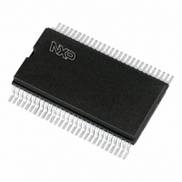
PCF8579T/1,112 NXP Semiconductors, PCF8579T/1,112 Datasheet - Page 8

PCF8579T/1,112
Manufacturer Part Number
PCF8579T/1,112
Description
IC LCD DRIVER DOT MATRIX 56-VSOP
Manufacturer
NXP Semiconductors
Datasheet
1.PCF8579T1112.pdf
(41 pages)
Specifications of PCF8579T/1,112
Package / Case
56-VSOP
Display Type
LCD
Configuration
Dot Matrix
Interface
I²C
Current - Supply
9µA
Voltage - Supply
2.5 V ~ 6 V
Operating Temperature
-40°C ~ 85°C
Mounting Type
Surface Mount
Maximum Clock Frequency
10 KHz
Operating Supply Voltage
2.5 V to 6 V
Maximum Power Dissipation
400 mW
Maximum Operating Temperature
+ 85 C
Maximum Supply Current
50 mA
Minimum Operating Temperature
- 40 C
Lead Free Status / RoHS Status
Lead free / RoHS Compliant
Digits Or Characters
-
Lead Free Status / Rohs Status
Lead free / RoHS Compliant
Other names
568-3562-5
935278869112
PCF8579TD
935278869112
PCF8579TD
NXP Semiconductors
PCF8579_5
Product data sheet
8.2 Multiplexed LCD bias generation
V
V
Remark: Do not transfer data on the I
reset action to complete.
The bias levels required to produce maximum contrast depend on the multiplex rate and
the LCD threshold voltage (V
LCD exhibits 10 % contrast.
the discrimination ratios (D) for the different multiplex rates as functions of V
The RMS on-state voltage (V
and the RMS off-state voltage (V
where the values for n are determined by the multiplex rate (1:n). Valid values for n are:
Table 4.
V
Bias ratios
------------- -
V
------------- -
V
------------- -
V
------------- -
V
oper
off RMS
on RMS
n = 8 for 1:8 multiplex
n = 16 for 1:16 multiplex
n = 24 for 1:24 multiplex
n = 32 for 1:32 multiplex
V
V
V
V
oper
oper
oper
oper
2
3
4
5
=
V
=
=
DD
Optimum LCD voltages
V
V
–
oper
oper
V
LCD
1
-- -
n
------------------------------ -
Multiplex rate
1:8
0.739
0.522
0.478
0.261
2
+
n
------------------------
n
n 1
n
Rev. 05 — 11 May 2009
n 1
–
+
n
–
+
1
1
Table 4
2
th
on(RMS)
). V
off(RMS)
th
LCD column driver for dot matrix graphic displays
is typically defined as the RMS voltage at which the
) for the LCD is calculated with the equation
1:16
0.800
0.600
0.400
0.200
shows the optimum voltage bias levels and
2
C-bus for at least 1 ms after power-on to allow the
) with the equation
1:24
0.830
0.661
0.339
0.170
PCF8579
© NXP B.V. 2009. All rights reserved.
1:32
0.850
0.700
0.300
0.150
oper
.
Table 5
8 of 41
(1)
(2)
(3)


