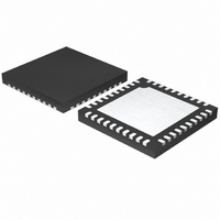
MAX6956ATL+ Maxim Integrated Products, MAX6956ATL+ Datasheet - Page 9

MAX6956ATL+
Manufacturer Part Number
MAX6956ATL+
Description
IC DRVR DSPL LED 40-TQFN
Manufacturer
Maxim Integrated Products
Datasheet
1.MAX6956AAI.pdf
(24 pages)
Specifications of MAX6956ATL+
Display Type
LED
Interface
I²C
Current - Supply
180µA
Voltage - Supply
2.5 V ~ 5.5 V
Operating Temperature
-40°C ~ 125°C
Mounting Type
Surface Mount
Package / Case
40-TQFN Exposed Pad
Number Of Segments
28
Low Level Output Current
18000 uA
Operating Supply Voltage
2.5 V to 5.5 V
Maximum Supply Current
270 uA
Maximum Power Dissipation
2105 mW
Maximum Operating Temperature
+ 125 C
Mounting Style
SMD/SMT
Minimum Operating Temperature
- 40 C
Lead Free Status / RoHS Status
Lead free / RoHS Compliant
Configuration
-
Digits Or Characters
-
Lead Free Status / Rohs Status
Lead free / RoHS Compliant
Figure 6. Slave Address
Figure 5. Acknowledge
MAX6956 is the recipient. When the MAX6956 is trans-
mitting to the master, the master generates the
acknowledge bit because the master is the recipient.
The MAX6956 has a 7-bit-long slave address (Figure 6).
The eighth bit following the 7-bit slave address is the
R/ W bit. It is low for a write command, high for a read
command.
The first 3 bits (MSBs) of the MAX6956 slave address
are always 100. Slave address bits A3, A2, A1, and A0
are selected by address inputs, AD1 and AD0. These
two input pins may be connected to GND, V+, SDA, or
SCL. The MAX6956 has 16 possible slave addresses
(Table 3) and therefore, a maximum of 16 MAX6956
devices may share the same interface.
A write to the MAX6956 comprises the transmission of
the MAX6956’s slave address with the R/ W bit set to
zero, followed by at least 1 byte of information. The first
BY TRANSMITTER
SDA
SCL
BY RECEIVER
28-Port LED Display Driver and I/O Expander
MSB
SDA
SDA
SCL
1
START CONDITION
2-Wire-Interfaced, 2.5V to 5.5V, 20-Port or
S
_______________________________________________________________________________________
Message Format for Writing
0
0
1
Slave Address
the MAX6956
A3
2
A2
byte of information is the command byte. The com-
mand byte determines which register of the MAX6956
is to be written by the next byte, if received. If a STOP
condition is detected after the command byte is
received, then the MAX6956 takes no further action
(Figure 8) beyond storing the command byte.
Any bytes received after the command byte are data
bytes. The first data byte goes into the internal register of
the MAX6956 selected by the command byte (Figure 9). If
multiple data bytes are transmitted before a STOP condi-
tion is detected, these bytes are generally stored in subse-
quent MAX6956 internal registers because the command
byte address generally autoincrements (Table 4).
The MAX6956 is read using the MAX6956’s internally
stored command byte as address pointer, the same
way the stored command byte is used as address
pointer for a write. The pointer generally autoincre-
ments after each data byte is read using the same rules
as for a write (Table 4). Thus, a read is initiated by first
configuring the MAX6956’s command byte by perform-
A1
CLOCK PULSE FOR ACKNOWLEDGMENT
Message Format for Reading
LSB
A0
8
R/W
9
ACK
9


