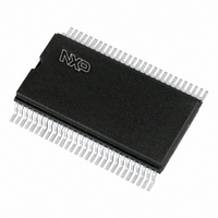
PCF8576CT/1,112 NXP Semiconductors, PCF8576CT/1,112 Datasheet - Page 16

PCF8576CT/1,112
Manufacturer Part Number
PCF8576CT/1,112
Description
IC LCD DVR UNVRSL LOW-MUX 56VSOP
Manufacturer
NXP Semiconductors
Specifications of PCF8576CT/1,112
Package / Case
56-VSOP
Display Type
LCD
Configuration
40 Segment
Interface
I²C
Current - Supply
120µA
Voltage - Supply
2 V ~ 6 V
Operating Temperature
-40°C ~ 85°C
Mounting Type
Surface Mount
Number Of Digits
20
Number Of Segments
160
Maximum Clock Frequency
315 KHz
Operating Supply Voltage
2 V to 6 V
Maximum Power Dissipation
400 mW
Maximum Operating Temperature
+ 85 C
Attached Touch Screen
No
Maximum Supply Current
120 uA
Minimum Operating Temperature
- 40 C
Lead Free Status / RoHS Status
Lead free / RoHS Compliant
Digits Or Characters
-
Lead Free Status / Rohs Status
Lead free / RoHS Compliant
Other names
935278818112
PCF8576CTD
PCF8576CTD
PCF8576CTD
PCF8576CTD
Philips Semiconductors
6.12
The addressing mechanism for the display RAM is
realized using the data pointer. This allows the loading of
an individual display data byte, or a series of display data
bytes, into any location of the display RAM. The sequence
commences with the initialization of the data pointer by the
LOAD DATA POINTER command. Following this, an
arriving data byte is stored starting at the display RAM
address indicated by the data pointer thereby observing
the filling order shown in Fig.11. The data pointer is
automatically incremented in accordance with the chosen
LCD configuration. That is, after each byte is stored, the
contents of the data pointer are incremented by eight
(static drive mode), by four (1 : 2 multiplex drive mode) or
by two (1 : 4 multiplex drive mode).
6.13
The storage of display data is conditioned by the contents
of the subaddress counter. Storage is allowed to take
place only when the contents of the subaddress counter
agree with the hardware subaddress applied to A0, A1
and A2. The subaddress counter value is defined by the
DEVICE SELECT command. If the contents of the
subaddress counter and the hardware subaddress do not
agree then data storage is inhibited but the data pointer is
incremented as if data storage had taken place. The
subaddress counter is also incremented when the data
pointer overflows.
The storage arrangements described lead to extremely
efficient data loading in cascaded applications. When a
series of display bytes are sent to the display RAM,
automatic wrap-over to the next PCF8576 occurs when
the last RAM address is exceeded. Subaddressing across
device boundaries is successful even if the change to the
next device in the cascade occurs within a transmitted
character (such as during the 14th display data byte
transmitted in 1 : 3 multiplex mode).
2001 Oct 02
Universal LCD driver for low multiplex rates
Data pointer
Subaddress counter
16
6.14
This selects one of the four bits per display RAM address
for transfer to the display latch. The actual bit chosen
depends on the particular LCD drive mode in operation
and on the instant in the multiplex sequence. In 1 : 4
multiplex, all RAM addresses of bit 0 are the first to be
selected, these are followed by the contents of bit 1, bit 2
and then bit 3. Similarly in 1 : 3 multiplex, bits 0, 1 and 2
are selected sequentially. In 1 : 2 multiplex, bits 0 and 1
are selected and, in the static mode, bit 0 is selected.
The PCF8576 includes a RAM bank switching feature in
the static and 1 : 2 multiplex drive modes. In the static
drive mode, the BANK SELECT command may request
the contents of bit 2 to be selected for display instead of
bit 0 contents. In the 1 : 2 drive mode, the contents of
bits 2 and 3 may be selected instead of bits 0 and 1. This
gives the provision for preparing display information in an
alternative bank and to be able to switch to it once it is
assembled.
6.15
The input bank selector loads display data into the display
RAM in accordance with the selected LCD drive
configuration. Display data can be loaded in bit 2 in static
drive mode or in bits 2 and 3 in 1 : 2 drive mode by using
the BANK SELECT command. The input bank selector
functions independent of the output bank selector.
Output bank selector
Input bank selector
Product specification
PCF8576


