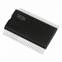
PCF8576CT/1,112 NXP Semiconductors, PCF8576CT/1,112 Datasheet - Page 20

PCF8576CT/1,112
Manufacturer Part Number
PCF8576CT/1,112
Description
IC LCD DVR UNVRSL LOW-MUX 56VSOP
Manufacturer
NXP Semiconductors
Specifications of PCF8576CT/1,112
Package / Case
56-VSOP
Display Type
LCD
Configuration
40 Segment
Interface
I²C
Current - Supply
120µA
Voltage - Supply
2 V ~ 6 V
Operating Temperature
-40°C ~ 85°C
Mounting Type
Surface Mount
Number Of Digits
20
Number Of Segments
160
Maximum Clock Frequency
315 KHz
Operating Supply Voltage
2 V to 6 V
Maximum Power Dissipation
400 mW
Maximum Operating Temperature
+ 85 C
Attached Touch Screen
No
Maximum Supply Current
120 uA
Minimum Operating Temperature
- 40 C
Lead Free Status / RoHS Status
Lead free / RoHS Compliant
Digits Or Characters
-
Lead Free Status / Rohs Status
Lead free / RoHS Compliant
Other names
935278818112
PCF8576CTD
PCF8576CTD
PCF8576CTD
PCF8576CTD
NXP Semiconductors
PCF8576C
Product data sheet
The display RAM bit map
backplane outputs BP0 to BP3, and the columns 0 to 39 which correspond with the
segment outputs S0 to S39. In multiplexed LCD applications the segment data of the first,
second, third and fourth row of the display RAM are time-multiplexed with BP0, BP1, BP2,
and BP3 respectively.
When display data is transmitted to the PCF8576C, the display bytes received are stored
in the display RAM in accordance with the selected LCD drive mode. The data is stored as
it arrives and does not wait for an acknowledge cycle as with the commands. Depending
on the current multiplex drive mode, data is stored singularly, in pairs, triples or
quadruples. To illustrate the filling order, an example of a 7-segment numeric display
showing all drive modes is given in
applies equally to other LCD types.
Fig 13. Display RAM bit map
backplane outputs
display RAM bits
The display RAM bitmap shows the direct relationship between the display RAM column and the
segment outputs; and between the bits in a RAM row and the backplane outputs.
(rows)/
(BP)
All information provided in this document is subject to legal disclaimers.
0
1
2
3
Rev. 10 — 22 July 2010
0
Figure 13
1
2
display RAM addresses (columns)/segment outputs (S)
Figure
3
shows the rows 0 to 3 which correspond with the
4
Universal LCD driver for low multiplex rates
14; the RAM filling organization depicted
35
PCF8576C
36
© NXP B.V. 2010. All rights reserved.
37
38
mbe525
39
20 of 57


