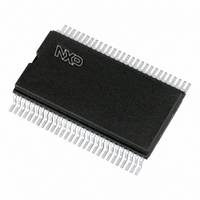
PCF8578T/1,118 NXP Semiconductors, PCF8578T/1,118 Datasheet - Page 19

PCF8578T/1,118
Manufacturer Part Number
PCF8578T/1,118
Description
IC LCD DRIVER ROW/COLUMN 56-VSOP
Manufacturer
NXP Semiconductors
Specifications of PCF8578T/1,118
Package / Case
56-VSOP
Display Type
LCD
Configuration
Dot Matrix
Interface
I²C
Voltage - Supply
2.5 V ~ 6 V
Operating Temperature
-40°C ~ 85°C
Mounting Type
Surface Mount
Number Of Digits
24
Number Of Segments
7
Maximum Clock Frequency
3.3 KHz
Operating Supply Voltage
2.5 V to 6 V
Maximum Power Dissipation
400 mW
Maximum Operating Temperature
+ 150 C
Attached Touch Screen
No
Maximum Supply Current
50 mA
Minimum Operating Temperature
- 65 C
Lead Free Status / RoHS Status
Lead free / RoHS Compliant
Current - Supply
-
Digits Or Characters
-
Lead Free Status / Rohs Status
Details
Other names
935278868118
PCF8578TD-T
PCF8578TD-T
PCF8578TD-T
PCF8578TD-T
Available stocks
Company
Part Number
Manufacturer
Quantity
Price
Part Number:
PCF8578T/1,118
Manufacturer:
NXP/恩智浦
Quantity:
20 000
Philips Semiconductors
8
Two 7-bit slave addresses (0111100 and 0111101) are
reserved for both the PCF8578 and PCF8579. The least
significant bit of the slave address is set by connecting
input SA0 to either 0 (V
of PCF8578 or PCF8579 can be distinguished on the
same I
1. One PCF8578 to operate with up to 32 PCF8579s on
2. The use of two types of LCD multiplex schemes on the
In most applications the PCF8578 will have the same slave
address as the PCF8579.
The I
All communications are initiated with a start condition (S)
from the I
slave address and read/write bit. All devices with this slave
address acknowledge in parallel. All other devices ignore
the bus transfer.
In WRITE mode (indicated by setting the read/write bit
LOW) one or more commands follow the slave address
acknowledgement. The commands are also
acknowledged by all addressed devices on the bus.
The last command must clear the continuation bit C.
After the last command a series of data bytes may follow.
The acknowledgement after each byte is made only by the
(A0, A1, A2 and A3) addressed PCF8579 or PCF8578
with its implicit subaddress 0. After the last data byte
has been acknowledged, the I
condition (P).
2003 Apr 14
LCD row/column driver for
dot matrix graphic displays
the same I
same I
I
2
2
C-BUS PROTOCOL
C-bus protocol is shown in Fig.13.
2
C-bus which allows:
2
C-bus master, which is followed by the desired
2
C-bus.
2
C-bus for very large applications
SS
) or 1 (V
2
C-bus master issues a stop
DD
). Therefore, two types
19
In READ mode, indicated by setting the read/write bit
HIGH, data bytes may be read from the RAM following the
slave address acknowledgement. After this
acknowledgement the master transmitter becomes a
master receiver and the PCF8578 becomes a slave
transmitter. The master receiver must acknowledge the
reception of each byte in turn. The master receiver must
signal an end of data to the slave transmitter, by not
generating an acknowledge on the last byte clocked out of
the slave. The slave transmitter then leaves the data line
HIGH, enabling the master to generate a stop condition
(P).
Display bytes are written into, or read from, the RAM at the
address specified by the data pointer and subaddress
counter. Both the data pointer and subaddress counter are
automatically incremented, enabling a stream of data to be
transferred either to, or from, the intended devices.
In multiple device applications, the hardware subaddress
pins of the PCF8579s (A0 to A3) are connected to V
V
If two or more devices share the same slave address, then
each device must be allocated a unique hardware
subaddress.
DD
to represent the desired hardware subaddress code.
Product specification
PCF8578
SS
or


