MAX6960ATH+ Maxim Integrated Products, MAX6960ATH+ Datasheet - Page 5
MAX6960ATH+
Manufacturer Part Number
MAX6960ATH+
Description
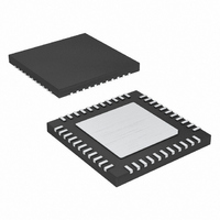
IC DRVR LED 8X8 44-TQFN
Manufacturer
Maxim Integrated Products
Datasheet
1.MAX6963ATH.pdf
(35 pages)
Specifications of MAX6960ATH+
Display Type
LED
Configuration
8 x 8 (Matrix)
Interface
4-Wire Serial
Digits Or Characters
Any Digit Type
Current - Supply
7.5mA
Voltage - Supply
2.7 V ~ 3.6 V
Operating Temperature
-40°C ~ 125°C
Mounting Type
Surface Mount
Package / Case
44-TQFN Exposed Pad
Number Of Segments
64
Low Level Output Current
750000 uA
High Level Output Current
48000 uA
Operating Supply Voltage
2.7 V to 3.6 V
Maximum Supply Current
11 mA
Maximum Power Dissipation
2162 mW
Maximum Operating Temperature
+ 125 C
Mounting Style
SMD/SMT
Minimum Operating Temperature
- 40 C
Lead Free Status / RoHS Status
Lead free / RoHS Compliant


2–5, 7–10 2–5, 7–10
1, 6, 11,
19, 20,
23–27,
29–33,
35, 36,
22, 28,
MQFP
12, 44
34, 38
21,
13
14
15
16
17
18
37
39
40
41
42
43
—
PIN
1, 6, 11,
19, 20,
35, 36,
22, 28,
23–27,
29–33,
12, 44
34, 38
TQFN
21,
EP
13
14
15
16
17
18
37
39
40
41
42
43
_______________________________________________________________________________________
ROW1–ROW8
COL1–COL16
ADDOUT
ADDCLK
ADDIN
RISET0
RISET1
NAME
DOUT
GND
OSC
CLK
DIN
RST
CS
V+
EP
8 x 8 Matrix Graphic LED Drivers
Ground
LE D C athod e D r i ver s. ROW 1 to RO W 8 outp uts si nk cur r ent fr om the d i sp l ay' s cathod e r ow s.
Multiplex Clock Input. Drive OSC with a 1MHz to 8.5MHz CMOS clock.
Chip-Select Input. Serial data is loaded into the shift register when CS is low. Data is
loaded into the data latch on CS's rising edge.
Serial-Data Input. Data from DIN loads into the internal shift register on CLK's rising edge.
Serial-Data Output. The output is tri-state.
Serial-Clock Input. On CLK's rising edge data shifts into the internal shift register.
Reset Input. Hold RST low until at least 50ms after all interconnected MAX6960s are
powered up.
LED Anode Drivers. COL1 to COL16 outputs source current into the display's anode
columns.
Positive Supply Voltage. Bypass V+ to GND with a single 47µF bulk capacitor per chip
plus a 0.1µF ceramic capacitor per V+.
Address-Data Output. Connect ADDOUT to ADDIN of the next MAX6960. Use ADDOUT of
the last MAX6960 as a plane change interrupt output.
Address-Data Input. For first MAX6960, connect ADDIN to V+. For other MAX6960s,
connect ADDIN to ADDOUT of the preceding MAX6960.
Address-Clock Input/Output. Connect ADDCLK of all MAX6960 drivers together, ensuring
that only one MAX6960's ADDIN input is connected to V+.
Digit 0 Current Setting. Connect RISET0 to GND to program all of digit 0's segment
currents to 40mA. Leave RISET0 open circuit to program all of digit 0's segment currents
to 20mA. Connect RISET0 to GND through a fixed or variable resistor to adjust all of digit
0's segment currents between 20mA and 40mA.
Digit 1 Current Setting. Connect RISET1 to GND to program all of digit 1's segment
currents to 40mA. Leave RISET1 open circuit to program all of digit 1's segment currents
to 20mA. Connect RISET1 to GND through a fixed or variable resistor to adjust all of digit
1's segment currents between 20mA and 40mA.
Exposed Pad on Package Underside. Connect to GND.
4-Wire Serially Interfaced
FUNCTION
Pin Description
5
Related parts for MAX6960ATH+
Image
Part Number
Description
Manufacturer
Datasheet
Request
R

Part Number:
Description:
4-Wire Serially Interfaced 8 x 8 Matrix Graphic LED Drivers
Manufacturer:
MAXIM [Maxim Integrated Products]
Datasheet:
Part Number:
Description:
Microprocessor Supervisory Circuits
Manufacturer:
MAXIM [Maxim Integrated Products]
Datasheet:

Part Number:
Description:
MAX7528KCWPMaxim Integrated Products [CMOS Dual 8-Bit Buffered Multiplying DACs]
Manufacturer:
Maxim Integrated Products
Datasheet:
Part Number:
Description:
Single +5V, fully integrated, 1.25Gbps laser diode driver.
Manufacturer:
Maxim Integrated Products
Datasheet:
Part Number:
Description:
Single +5V, fully integrated, 155Mbps laser diode driver.
Manufacturer:
Maxim Integrated Products
Datasheet:
Part Number:
Description:
VRD11/VRD10, K8 Rev F 2/3/4-Phase PWM Controllers with Integrated Dual MOSFET Drivers
Manufacturer:
Maxim Integrated Products
Datasheet:
Part Number:
Description:
Highly Integrated Level 2 SMBus Battery Chargers
Manufacturer:
Maxim Integrated Products
Datasheet:
Part Number:
Description:
Current Monitor and Accumulator with Integrated Sense Resistor; ; Temperature Range: -40°C to +85°C
Manufacturer:
Maxim Integrated Products
Part Number:
Description:
TSSOP 14/A°/RS-485 Transceivers with Integrated 100O/120O Termination Resis
Manufacturer:
Maxim Integrated Products
Part Number:
Description:
TSSOP 14/A°/RS-485 Transceivers with Integrated 100O/120O Termination Resis
Manufacturer:
Maxim Integrated Products
Part Number:
Description:
QFN 16/A°/AC-DC and DC-DC Peak-Current-Mode Converters with Integrated Step
Manufacturer:
Maxim Integrated Products
Part Number:
Description:
TDFN/A/65V, 1A, 600KHZ, SYNCHRONOUS STEP-DOWN REGULATOR WITH INTEGRATED SWI
Manufacturer:
Maxim Integrated Products
Part Number:
Description:
Integrated Temperature Controller f
Manufacturer:
Maxim Integrated Products
Part Number:
Description:
SOT23-6/I°/45MHz to 650MHz, Integrated IF VCOs with Differential Output
Manufacturer:
Maxim Integrated Products
Part Number:
Description:
SOT23-6/I°/45MHz to 650MHz, Integrated IF VCOs with Differential Output
Manufacturer:
Maxim Integrated Products