LM3915N National Semiconductor, LM3915N Datasheet - Page 6
LM3915N
Manufacturer Part Number
LM3915N
Description
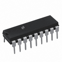
IC DRIVER DOT BAR DISPLAY 18-DIP
Manufacturer
National Semiconductor
Datasheet
1.LM3915N.pdf
(20 pages)
Specifications of LM3915N
Display Type
LED, LCD, Vacuum Fluorescent
Configuration
Dot/Bar Display
Digits Or Characters
10 Steps
Current - Supply
6.1mA
Voltage - Supply
3 V ~ 25 V
Operating Temperature
0°C ~ 70°C
Mounting Type
Through Hole
Package / Case
18-DIP (0.300", 7.62mm)
Lead Free Status / RoHS Status
Contains lead / RoHS non-compliant
Interface
-
Other names
*LM3915N
LM3915
LM3915
Available stocks
Company
Part Number
Manufacturer
Quantity
Price

Part Number:
LM3915N
Manufacturer:
NS/国半
Quantity:
20 000
Company:
Part Number:
LM3915N-1
Manufacturer:
TI
Quantity:
13 000
Part Number:
LM3915N-1
Manufacturer:
NS/国半
Quantity:
20 000
Part Number:
LM3915N-1/NOPB
Manufacturer:
NS/国半
Quantity:
20 000


Functional Description
The simplified LM3915 block diagram is included to give the
general idea of the circuit’s operation A high input imped-
ance buffer operates with signals from ground to 12V and is
protected against reverse and overvoltage signals The sig-
nal is then applied to a series of 10 comparators each of
which is biased to a different comparison level by the resis-
tor string
In the example illustrated the resistor string is connected to
the internal 1 25V reference voltage In this case for each
3 dB that the input signal increases a comparator will
switch on another indicating LED This resistor divider can
be connected between any 2 voltages providing that they
are at least 1 5V below V
INTERNAL VOLTAGE REFERENCE
The reference is designed to be adjustable and develops a
nominal 1 25V between the REF OUT (pin 7) and REF ADJ
(pin 8) terminals The reference voltage is impressed across
program resistor R1 and since the voltage is constant a
constant current I
tor R2 giving an output voltage of
Since the 120
represents an error term the reference was designed to
minimize changes of this current with V
For correct operation reference load current should be be-
tween 80
than 0 05 F
CURRENT PROGRAMMING
A feature not completely illustrated by the block diagram is
the LED brightness control The current drawn out of the
reference voltage pin (pin 7) determines LED current Ap-
proximately 10 times this current will be drawn through each
lighted LED and this current will be relatively constant de-
spite supply voltage and temperature changes Current
drawn by the internal 10-resistor divider as well as by the
external current and voltage-setting divider should be in-
cluded in calculating LED drive current The ability to modu-
late LED brightness with time or in proportion to input volt-
age and other signals can lead to a number of novel dis-
plays or ways of indicating input overvoltages alarms etc
The LM3915 outputs are current-limited NPN transistors as
shown below An internal feedback loop regulates the tran-
sistor drive Output current is held at about 10 times the
reference load current independent of output voltage and
processing variables as long as the transistor is not saturat-
ed
V
A and 5 mA Load capacitance should be less
OUT
A current (max) from the adjust terminal
e
1
then flows through the output set resis-
V
REF
a
and no lower than V
1
a
R2
R1
a
a
I
ADJ
and load changes
R2
b
TL H 5104– 5
6
Outputs may be run in saturation with no adverse effects
making it possible to directly drive logic The effective satu-
ration resistance of the output transistors equal to R
the transistors’ collector resistance is about 50
possible to drive LEDs from rectified AC with no filtering To
avoid oscillations the LED supply should be bypassed with
a 2 2 F tantalum or 10 F aluminum electrolytic capacitor
MODE PIN USE
Pin 9 the Mode Select input permits chaining of multiple
LM3915s and controls bar or dot mode operation The fol-
lowing tabulation shows the basic ways of using this input
Other more complex uses will be illustrated in the applica-
tions
Bar Graph Display Wire Mode Select (pin 9) directly to pin
3 (V
Dot Display Single LM3915 Driver Leave the Mode Se-
lect pin open circuit
Dot Display 20 or More LEDs Connect pin 9 of the first
driver in the series (i e the one with the lowest input volt-
age comparison points) to pin 1 of the next higher LM3915
driver Continue connecting pin 9 of lower input drivers to
pin 1 of higher input drivers for 30 or more LED displays
The last LM3915 driver in the chain will have pin 9 left open
All previous drivers should have a 20k resistor in parallel
with LED
Mode Pin Functional Description
This pin actually performs two functions Refer to the simpli-
fied block diagram below
a
pin)
Block Diagram of Mode Pin Function
9 (pin 11 to V
LM3915 Output Circuit
LED
)
High for bar
TL H 5104 – 6
TL H 5104 – 7
It’s also
E
plus
Related parts for LM3915N
Image
Part Number
Description
Manufacturer
Datasheet
Request
R

Part Number:
Description:
Audio Power Driver (discontinued)
Manufacturer:
National Semiconductor Corporation
Datasheet:

Part Number:
Description:
National Semiconductor [8-Bit D/A Converter]
Manufacturer:
National Semiconductor
Datasheet:
Part Number:
Description:
National Semiconductor [Media Coprocessor]
Manufacturer:
National Semiconductor
Datasheet:
Part Number:
Description:
Digitally Controlled Tone and Volume Circuit with Stereo Audio Power Amplifier, Microphone Preamp Stage and National 3D Sound
Manufacturer:
National Semiconductor
Datasheet:
Part Number:
Description:
Digitally Controlled Tone and Volume Circuit with Stereo Audio Power Amplifier, Microphone Preamp Stage and National 3D Sound
Manufacturer:
National Semiconductor
Datasheet:
Part Number:
Description:
AC97 Rev 2 Codec with Sample Rate Conversion and National 3D Sound
Manufacturer:
National Semiconductor
Part Number:
Description:
Manufacturer:
National Semiconductor
Datasheet:
Part Number:
Description:
Manufacturer:
National Semiconductor
Datasheet:
Part Number:
Description:
General Purpose, Low Voltage, Low Power, Rail-to-Rail Output Operational Amplifiers
Manufacturer:
National Semiconductor
Datasheet:
Part Number:
Description:
8-bit 20 MSPS flash A/D converter.
Manufacturer:
National Semiconductor
Datasheet:
Part Number:
Description:
Low Noise Quad Operational Amplifier
Manufacturer:
National Semiconductor
Datasheet:
Part Number:
Description:
Quad Differential Line Receivers
Manufacturer:
National Semiconductor
Datasheet:
Part Number:
Description:
Quad High Speed Trapezoidal? Bus Transceiver
Manufacturer:
National Semiconductor
Datasheet:
Part Number:
Description:
Dual Line Receiver
Manufacturer:
National Semiconductor
Datasheet: