LM2402T National Semiconductor, LM2402T Datasheet - Page 4
LM2402T
Manufacturer Part Number
LM2402T
Description
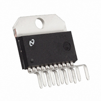
IC DRIVER MONOLITHIC TO-220-11
Manufacturer
National Semiconductor
Datasheet
1.LM2402T.pdf
(11 pages)
Specifications of LM2402T
Display Type
CRT
Current - Supply
27mA
Voltage - Supply
60 V ~ 85 V
Operating Temperature
-20°C ~ 100°C
Mounting Type
Through Hole
Package / Case
TO-220-11 (Bent and Staggered Leads)
Lead Free Status / RoHS Status
Contains lead / RoHS non-compliant
Interface
-
Configuration
-
Digits Or Characters
-
Other names
*LM2402T
Available stocks
Company
Part Number
Manufacturer
Quantity
Price

Part Number:
LM2402T
Manufacturer:
NS/国半
Quantity:
20 000


www.national.com
Theory of Operation
The LM2402 is a high voltage monolithic three channel CRT
driver suitable for very high resolution display applications,
up to 1600 x 1200 at 85 Hz refresh rate. The LM2402 oper-
ates using 80V and 12V power supplies. The part is housed
in the industry standard 11-lead TO-220 molded plastic
power package.
The simplified circuit diagram of one channel of the LM2402
is shown in Figure 1 . A PNP emitter follower, Q5, provides in-
put buffering. This minimizes the current loading of the video
pre-amp. R9 is used to turn off Q5 when there is no input.
This will drive the output stage to the V
power dissipation with no inputs. R6 is a pull-up resistor for
Q5 and also limits the current flow through Q5. R3 and R2
are used to set the current flow through Q1 and Q2. The ratio
of R1 to R2 is used to set the gain of the LM2402. R1, R2
and R3 are all related when calculating the output voltage of
the CRT driver. R
Q1 and Q2 are in a cascade configuration. Q1 is a low volt-
age and very fast transistor. Q2 is a higher voltage transistor.
The cascade configuration gives the equivalent of a very fast
and high voltage transistor. The two output transistors, Q3
and Q4, form a class B amplifier output stage. R4 and R5 are
used to limit the current through the output stage and set the
output impedance of the LM2402. Q6, along with R7 and R8
set the bias current through Q3 and Q4 when there is no
change in the signal level. This bias current minimizes the
crossover distortion of the output stage. With this bias cur-
rent the output stage now becomes a class AB amplifier with
a crossover distortion much lower than a class B amplifier.
Figure 2 shows a typical test circuit for evaluation of the
LM2402. Due to the very wide bandwidth of the LM2402, it is
necessary to use a FET probe that is DC coupled to the out-
put for evaluation of the CRT driver’s performance. The 50
resistor is used to duplicate the required series resistor in the
actual application. This resistor would be part of the arc-over
protection circuit. The input signal from the generator is AC
coupled to the input of the CRT driver.
Application Hints
INTRODUCTION
National Semiconductor (NSC) is committed to providing ap-
plication information that assists our customers in obtaining
the best performance possible from our products. The follow-
ing information is provided in order to support this commit-
ment. The reader should be aware that the optimization of
performance was done using a specific printed circuit board
designed at NSC. Variations in performance can be realized
due to physical changes in the printed circuit board and the
application. Therefore, the designer should know that com-
ponent value changes may be required in order to optimize
performance in a given application. The values shown in this
document can be used as a starting point for evaluation pur-
poses. When working with high bandwidth circuits, good lay-
out practices are also critical to achieving maximum perfor-
mance.
POWER SUPPLY BYPASS
Since the LM2402 is a very high bandwidth amplifier, proper
power supply bypassing is critical for optimum performance.
Improper power supply bypassing can result in large over-
shoot, ringing and oscillation. A 0.1 µF capacitor should be
connected from the supply pin, V
the supply and ground pins as is practical. Additionally, a
b
limits the current through the base of Q2.
CC
, to ground, as close to
CC
rail, minimizing the
4
10 µF to 100 µF electrolytic capacitor should be connected
from the supply pin to ground. The electrolytic capacitor
should also be placed reasonably close to the LM2402’s
supply and ground pins. A 0.1 µF capacitor should be con-
nected from the bias pin, V
tical to the part.
ARC PROTECTION
During normal CRT operation, internal arcing may occasion-
ally occur. Spark gaps, in the range of 200V, connected from
the CRT cathodes to CRT ground will limit the maximum volt-
age, but to a value that is much higher than allowable on the
LM2402. This fast, high voltage, high energy pulse can dam-
age the LM2402 output stage. The application circuit shown
in Figure 9 is designed to help clamp the voltage at the out-
put of the LM2402 to a safe level. The clamp diodes should
have a fast transient response, high peak current rating, low
series impedance and low shunt capacitance. FDH400 or
equivalent diodes are recommended. D1 and D2 should
have short, low impedance connections to V
respectively. The cathode of D1 should be located very close
to a separately decoupled bypass capacitor. The ground
connection of the diode and the decoupling capacitor should
be very close to the LM2402 ground. This will significantly re-
duce the high frequency voltage transients that the LM2402
would be subjected to during an arc-over condition. Resistor
R2 limits the arc-over current that is seen by the diodes while
R1 limits the current into the LM2402 as well as the voltage
stress at the outputs of the device. R2 should be a
carbon type resistor. R1 can be a
type resistor. Inductor L1 is critical to reduce the initial high
frequency voltage levels that the LM2402 would be sub-
jected to during an arc-over. Having large value resistors for
R1 and R2 would be desirable, but this has the effect of in-
creasing rise and fall times. The inductor will not only help
protect the device but it will also help optimize rise and fall
times as well as minimize EMI. For proper arc protection, it is
important to not omit any of the arc protection components
shown in Figure 9 . The values of L1 and R1 may need to be
adjusted for a particular application. The recommended mini-
mum value for R1 is 43 , with L1 = .049 µH.
OPTIMIZING TRANSIENT RESPONSE
Referring to Figure 9 , there are three components (R1, R2
and L1) that can be adjusted to optimize the transient re-
sponse of the application circuit. Increasing the values of R1
and R2 will slow the circuit down while decreasing over-
shoot. Increasing the value of L1 will speed up the circuit as
well as increase overshoot. It is very important to use induc-
tors with very high self-resonant frequencies, preferably
above 300 MHz. Air core inductors from J.W. Miller Magnet-
ics (part #75F518MPC) were used for optimizing the perfor-
FIGURE 9. One Channel of the LM2402 with the
Recommended Arc Protection Circuit.
BB
, to ground, as close as is prac-
1
⁄
4
W metal or carbon film
CC
and ground
1
DS101016-10
⁄
2
W solid
Related parts for LM2402T
Image
Part Number
Description
Manufacturer
Datasheet
Request
R

Part Number:
Description:
Monolithic Triple 3 ns CRT Driver
Manufacturer:
National Semiconductor
Datasheet:
Part Number:
Description:
National Semiconductor [8-Bit D/A Converter]
Manufacturer:
National Semiconductor
Datasheet:
Part Number:
Description:
National Semiconductor [Media Coprocessor]
Manufacturer:
National Semiconductor
Datasheet:
Part Number:
Description:
Digitally Controlled Tone and Volume Circuit with Stereo Audio Power Amplifier, Microphone Preamp Stage and National 3D Sound
Manufacturer:
National Semiconductor
Datasheet:
Part Number:
Description:
Digitally Controlled Tone and Volume Circuit with Stereo Audio Power Amplifier, Microphone Preamp Stage and National 3D Sound
Manufacturer:
National Semiconductor
Datasheet:
Part Number:
Description:
AC97 Rev 2 Codec with Sample Rate Conversion and National 3D Sound
Manufacturer:
National Semiconductor
Part Number:
Description:
Manufacturer:
National Semiconductor
Datasheet:
Part Number:
Description:
Manufacturer:
National Semiconductor
Datasheet:
Part Number:
Description:
General Purpose, Low Voltage, Low Power, Rail-to-Rail Output Operational Amplifiers
Manufacturer:
National Semiconductor
Datasheet:
Part Number:
Description:
8-bit 20 MSPS flash A/D converter.
Manufacturer:
National Semiconductor
Datasheet:
Part Number:
Description:
Low Noise Quad Operational Amplifier
Manufacturer:
National Semiconductor
Datasheet:
Part Number:
Description:
Quad Differential Line Receivers
Manufacturer:
National Semiconductor
Datasheet:
Part Number:
Description:
Quad High Speed Trapezoidal? Bus Transceiver
Manufacturer:
National Semiconductor
Datasheet:
Part Number:
Description:
Dual Line Receiver
Manufacturer:
National Semiconductor
Datasheet: